三菱ケミカル:大口径GaN単結晶基板を量産:2、4、6インチ基板(動画):
Mitsubishi Chem: Large-diameter GaN single crystal substrates:2,4,6-inch:
三菱化学:量产大口径GaN单晶衬底:2、4、6英寸衬底
ー次世代EV技術・非接触充電を実現ー
三菱ケミカル:
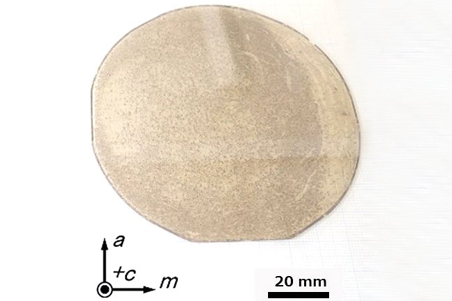
三菱ケミカルが、大口径のGaN単結晶基板量産化にめどを付けた。
EV非接触充電技術を実現:
走行中に電気自動車(EV)を非接触充電する次世代EV技術が実現に近づいてきた。
GaN単結晶基板:
- GaN単結晶基板は、
- より大電流での動作が可能、
- 高耐圧パワー半導体を実現、
電子機器などを効率化、小型化できる。
新素材が、EVの新たな可能性を切り開く。
三菱ケミカル:
藤戸健史氏:
- 走行中のEV非接触充電システムや、
- 駆動用インホイールモーターでは、
- GaNオンGaNが必須になる。
基板生産設備を設置:
三菱ケミカルは、日本製鋼所と共同で、北海道室蘭市に、
2、4、6インチの基板を生産できる量産設備を設置した。
2022年度初頭から市場へ供給を始める。
液相成長法を採用:
「液相成長法」をこの設備で採用した。
従来の気相成長に比べ、欠陥密度を100分の1から1000分の1に抑えられる。
液相成長法の実現には、製造条件の大きなブレークスルーが必要。
液相成長法の開発に、約10年を要した。
単結晶を再析出:
- 液相成長法は、高温高圧下で、
- 超臨界状態にした液体アンモニアに、
- GaN多結晶を溶かし、
そこから単結晶を再析出させる。
従来:
GaNを溶かすため2000気圧に高めていたが、大型装置はこの気圧に耐えられない。今回:
三菱ケミカルは、アンモニアの添加鉱化剤を工夫、1000気圧下で大量のGaNが溶けるようにした(藤戸氏)日本製鋼所と協力:
「1000気圧に対応する大型装置の開発」は極めて難しい。
「水晶の結晶合成技術や大型装置技術を持つ日本製鋼所との協力」で、実現できた。
利用分野:
液相法による大口径化で、デバイス進化に貢献することが期待される。
次世代EV技術や、
モーターの小型化、
高出力・高輝度な光源、
情報通信分野、ニュースイッチ
Completion of the world’s largest manufacturing facility for gallium nitride (GaN) substrates
The Japan Steel Works, LTD.
Mitsubishi Chemical Corporation
have completed construction of a demonstration facility for mass production of gallium nitride (GaN) single-crystal substrates in the premises of the Muroran Plant of Japan Steel Works in collaboration.
We will conduct verification tests for mass production of 4-inch GaN single-crystal substrates throughout FY2021, and start market supply FY2022. 1.
Background GaN is a material used to create ultra-high-efficiency devices,
employing its enhanced efficiency and durability.
In addition, it is expected to have an environmental benefit
since the material can reduce CO2 emissions with a drastic reduction of power consumption.
Promising applications of GaN not only include blue LEDs
but the fields listed below as well:
1 High-power and high-intensity light source GaN is expected to be applied to high-intensity and high-power lasers, high-efficiency illumination, and new-generation displays.
2 Telecommunications GaN will contribute to 5th Generation Mobile Communication System (5G) such as high- frequency devices and optical communication devices that can
instantaneously transmit and
receive large amounts of data, and
even to post-5G. GaN,
with a higher processor frequency than currently prevailing silicone substrates, can also contribute to power saving of servers and base stations.
3 Power semiconductor In recent years, demands for power semiconductors that allow the downsizing of devices and instruments in particular have been increasing.
While silicone substrates currently predominate, demands for high-voltage power semiconductors that can attain higher-current operations are rising more than ever.
https://www.m-chemical.co.jp/en/news/2021/__icsFiles/afieldfile/2021/06/09/GaNeng.pdf