三菱化学:量产大口径GaN单晶衬底:2、4、6英寸衬底
-实现了下一代EV技术和非接触式充电-
三菱化学:
三菱化学对大直径GaN单晶衬底的量产寄予厚望。
EV非接触充电技术的实现:
可在驾驶时对电动汽车 (EV) 进行非接触式充电的下一代 EV 技术即将实现。
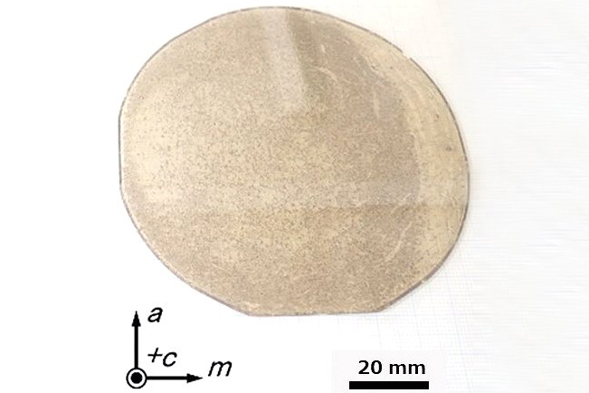
GaN单晶衬底:
GaN单晶衬底为
可以在更高的电流下工作,
实现高耐压功率半导体,
电子设备可以做得更高效、更小。
新材料为电动汽车开辟了新的可能性。
三菱化学:
藤户武:
EV 非接触式充电系统在行驶中,
用于驱动轮毂电机
需要 GaN 上的 GaN。
已安装板生产设备:
三菱化学与日本钢铁厂合作,在北海道室兰市,
安装了能够生产 2、4 和 6 英寸基板的批量生产设施。
市场供应将于 2022 年初开始。
采用液相生长法:
本设备采用“液相生长法”。
与传统的气相生长相比,缺陷密度可以抑制到 1/100 到 1/1000。
实现液相生长方法需要制造条件的重大突破。
开发液相生长方法大约需要10年时间。
单晶再沉淀:
液相生长法是在高温高压下进行的。
对于超临界状态的液氨,
熔化 GaN 多晶,
从那里,单晶被重新沉积。
传统的:
为了熔化GaN,它被提高到2000个大气压,但大型设备无法承受这种压力。
这次:
三菱化学为氨设计了一种添加剂矿化剂,以便在 1000 个大气压下可以溶解大量的 GaN(藤户先生)。
与日本钢厂的合作:
“开发可承受1000个大气压的大型装置”是极其困难的。
这是通过“与拥有石英晶体合成技术和大型设备技术的日本钢厂合作”实现的。
使用领域:
预计通过液相方法增加直径有助于设备的发展。
下一代电动汽车技术和
电机小型化,
高输出高亮度光源,
信息通信领域,
新开关
Completion of the world’s largest manufacturing facility for gallium nitride (GaN) substrates
The Japan Steel Works, LTD.
Mitsubishi Chemical Corporation
have completed construction of a demonstration facility for mass production of gallium nitride (GaN) single-crystal substrates in the premises of the Muroran Plant of Japan Steel Works in collaboration.
We will conduct verification tests for mass production of 4-inch GaN single-crystal substrates throughout FY2021, and start market supply FY2022. 1.
Background GaN is a material used to create ultra-high-efficiency devices,
employing its enhanced efficiency and durability.
In addition, it is expected to have an environmental benefit
since the material can reduce CO2 emissions with a drastic reduction of power consumption.
Promising applications of GaN not only include blue LEDs
but the fields listed below as well:
1 High-power and high-intensity light source GaN is expected to be applied to high-intensity and high-power lasers, high-efficiency illumination, and new-generation displays.
2 Telecommunications GaN will contribute to 5th Generation Mobile Communication System (5G) such as high- frequency devices and optical communication devices that can
instantaneously transmit and
receive large amounts of data, and
even to post-5G. GaN,
with a higher processor frequency than currently prevailing silicone substrates, can also contribute to power saving of servers and base stations.
3 Power semiconductor In recent years, demands for power semiconductors that allow the downsizing of devices and instruments in particular have been increasing.
While silicone substrates currently predominate, demands for high-voltage power semiconductors that can attain higher-current operations are rising more than ever.
https://www.m-chemical.co.jp/en/news/2021/__icsFiles/afieldfile/2021/06/09/GaNeng.pdf