Mitsubishi Chemical: Mass production of large-diameter GaN single crystal substrates: 2, 4, 6-inch substrates
-Achieves next-generation EV technology and non-contact charging-
Mitsubishi Chemical:
Mitsubishi Chemical has put the prospect in GaN single crystal substrate mass production of large diameter.
Realization of EV non-contact charging technology:
Next-generation EV technology that non-contactly charges electric vehicles (EVs) while driving is approaching realization.
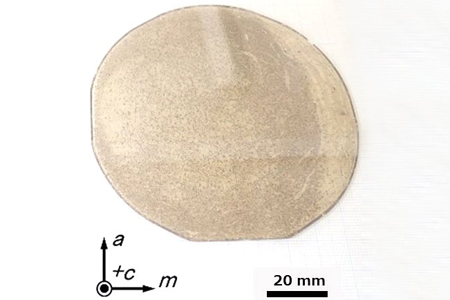
GaN single crystal substrate:
The GaN single crystal substrate is
Can operate with higher current,
Realizes high withstand voltage power semiconductors,
Electronic devices can be made more efficient and smaller.
New materials open up new possibilities for EVs.
Mitsubishi Chemical:
Takeshi Fujito:
EV non-contact charging system while driving,
For drive in-wheel motors
GaN on GaN is essential.
Installed board production equipment:
Mitsubishi Chemical, in collaboration with Japan Steel Works, in Muroran, Hokkaido,
A mass production facility capable of producing 2, 4 and 6 inch substrates was installed.
Supply to the market will begin in early 2022.
Adopted liquid phase growth method:
The “liquid phase growth method” was adopted in this equipment.
Compared with the conventional vapor phase growth, the defect density can be suppressed to 1/100 to 1/1000.
A major breakthrough in manufacturing conditions is required to realize the liquid phase growth method.
It took about 10 years to develop the liquid phase growth method.
Reprecipitation of single crystal:
The liquid phase growth method is performed under high temperature and high pressure.
For liquid ammonia in a supercritical state,
Melt a GaN polycrystal,
From there, the single crystal is redeposited.
Conventional:
It was raised to 2000 atm to melt GaN, but large equipment cannot withstand this pressure.
this time:
Mitsubishi Chemical has devised an additive mineralizing agent for ammonia so that a large amount of GaN can be dissolved under 1000 atm (Mr. Fujito).
Cooperation with Japan Steel Works:
“Development of a large device that can handle 1000 atmospheres” is extremely difficult.
This was achieved through “cooperation with Japan Steel Works, which has crystal synthesis technology for quartz and large equipment technology.”
Field of use:
It is expected to contribute to the evolution of devices by increasing the diameter by the liquid phase method.
Next-generation EV technology and
Motor miniaturization,
High output and high brightness light source,
Information and communication field,
New switch
Completion of the world’s largest manufacturing facility for gallium nitride (GaN) substrates
The Japan Steel Works, LTD.
Mitsubishi Chemical Corporation
have completed construction of a demonstration facility for mass production of gallium nitride (GaN) single-crystal substrates in the premises of the Muroran Plant of Japan Steel Works in collaboration.
We will conduct verification tests for mass production of 4-inch GaN single-crystal substrates throughout FY2021, and start market supply FY2022. 1.
Background GaN is a material used to create ultra-high-efficiency devices,
employing its enhanced efficiency and durability.
In addition, it is expected to have an environmental benefit
since the material can reduce CO2 emissions with a drastic reduction of power consumption.
Promising applications of GaN not only include blue LEDs
but the fields listed below as well:
1 High-power and high-intensity light source GaN is expected to be applied to high-intensity and high-power lasers, high-efficiency illumination, and new-generation displays.
2 Telecommunications GaN will contribute to 5th Generation Mobile Communication System (5G) such as high- frequency devices and optical communication devices that can
instantaneously transmit and
receive large amounts of data, and
even to post-5G. GaN,
with a higher processor frequency than currently prevailing silicone substrates, can also contribute to power saving of servers and base stations.
3 Power semiconductor In recent years, demands for power semiconductors that allow the downsizing of devices and instruments in particular have been increasing.
While silicone substrates currently predominate, demands for high-voltage power semiconductors that can attain higher-current operations are rising more than ever.
https://www.m-chemical.co.jp/en/news/2021/__icsFiles/afieldfile/2021/06/09/GaNeng.pdf