⚛AIST: Successful formation of large area of two-dimensional organic single-crystal nanosheet with only a few molecules
– High-speed organic integrated circuit substrate that can be printed –
Point of presentation
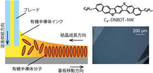
Organic semiconductors can be manufactured at low cost by a simple printing process, has been attracting attention as a next-generation electronic material, as compared to inorganic semiconductors such as silicon, it is difficult to a large area production of high quality single crystal, and very Has a large contact resistance, there was a problem that high-speed operation is difficult.
By simple printing technique using an organic semiconductor ink, developing a process for forming a film of large area 2-dimensional organic single crystal nanosheet consisting thickness of only a few molecular layers, organic field effect transistor using the same nanosheet (1) Achieved the world’s highest response frequency.
A high performance organic semiconductor capable of achieving both high mobility and low contact resistance was realized.
It opens the possibility of application of large scale integration circuit capable of high speed computation with organic semiconductors and is expected to be a fundamental technology to realize low cost film device which is responsible for IoT society.
The results of this research will be published in the science magazine “Science Advances” February 2,
http://www.aist.go.jp/aist_j/press_release/pr2018/pr20180203/pr20180203.html