Saga University: Successful mass production of 2-inch diamond wafers: Semiconductor power devices
-Achieved by a new principle using step flow growth-
September 9
Adamand Namiki Precision Jewel:
Developed a 2-inch diamond wafer mass production technology using a new principle of diamond crystal growth method.
Achieved the quality required for semiconductor devices.
Faculty of Science and Engineering, Saga University
Professor Makoto Kazu:
So far, as a joint research, we have developed our own method “microneedle method”.
Developed microneedle method
In the process of diamond layer crystal growth,
A diamond needle with a diameter of several μm and a length of several tens of μm,
A layered structure can be produced that is arranged at intervals of 10 μm.
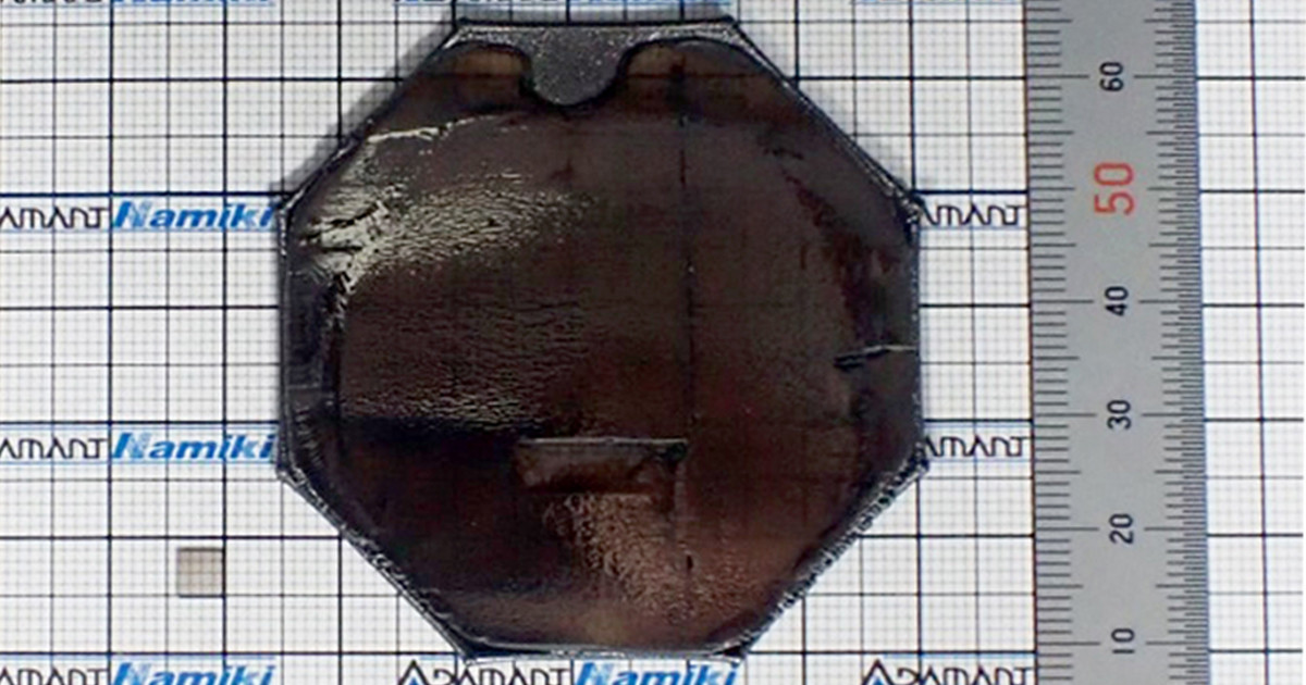
KENZAN Diamond:
Manufactured a 1-inch diamond wafer (trade name: KENZAN Diamond).
On the KENZAN wafer,
Based on a new operating principle,
Manufactures diamond semiconductor power devices.
It was reported in April 2021 that high output power characteristics had already been obtained.
Disadvantages of the microneedle method:
However, the microneedle method does not reach the 2 inches required for industrial applications.
The manufacturing process of the microneedle method is complicated and the manufacturing cost is high.
This time, using sapphire board:
So this time,
In Adamant Namiki Precision Jewels,
By “growing diamond crystals using a sapphire substrate”,
Succeeded in finding that the stress of the diamond film is reduced.
Achieved a large diameter with a sapphire substrate:
Diamond crystal growth was carried out using a sapphire substrate slightly inclined from the conventional crystal plane orientation.
By utilizing this technology,
Without using microneedles
It was confirmed that the diameter could be increased.
In the end, he said he succeeded in growing a 2-inch diamond wafer.
Power semiconductor characteristic measurement:
“Characteristics of a power semiconductor device made from a 2-inch diamond wafer” was measured.
Confirmed that it can output 345 MW / cm2 output power.
This research result:
September 13th at “82nd JSAP Autumn Meeting”
“High quality heteroepitaxial diamond using step flow growth”
Will be announced at.
TECH +
https://news.mynavi.jp/article/20210909-1968752/
Succeeded in mass production of diamond wafers for power semiconductors
-Commercialization in 2010 for adoption for 6G base stations-
Aim for research and mass production for larger diameters.
4-inch wafer in 2025
8-inch wafer in 2030Compare with GaN:
Diamond wafer power semiconductors
Compared to the case of using GaN
High output and excellent heat dissipation.For 6G communication base stations and EVs:
It is used for power control of 6G communication base stations and EVs.
New switch
Fabrication of diamond modulation-doped FETs by NO2 delta doping in an Al2O3 gate layer – IOPscience
https://iopscience.iop.org/article/10.35848/1882-0786/abf445