Osaka City University: Direct bonding of GaN and diamond: GaN-on-diamond
-Expected to improve the performance of GaN semiconductors-
Osaka City University:
The research group
GaN, the next-generation semiconductor material,
Diamond, which is said to be the ultimate semiconductor,
Succeeded in direct bonding at room temperature.
Osaka City University Graduate School
Tohoku University
Saga University
Adamant Namiki Precision Jewels, etc.
Collaboratively developed by the research group.
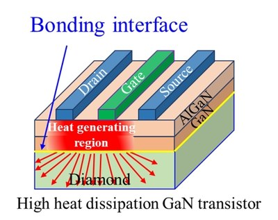
GaN-on-diamond:
Details were published in the international academic journal “ADVANCED MATERIALS”.
Research is underway to realize a GaN-on-diamond structure.
Conventional method:
In the conventional method, an intermediate layer is inserted between GaN and diamond.
Therefore, heat dissipation is hindered,
Insufficient crystallinity of diamond, etc.
The performance of diamond is not fully exhibited,
It is said that there was the above problem.
This method:
Aiming to solve such problems,
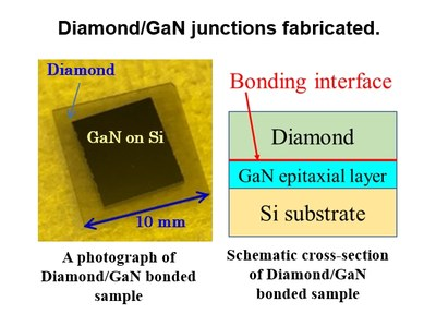
Accumulated on the Si substrate,
On the surface of a GaN thin layer with a thickness of about 1 μm,
A diamond substrate and surface activated bonding method are used.
With this, it is said that the direct coupling at room temperature was successful.
Result of normal temperature direct coupling:
After removing the Si substrate
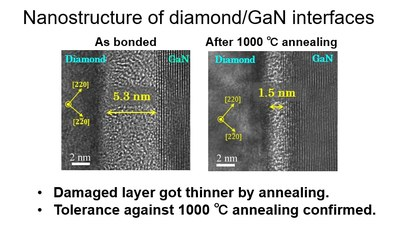
Heat treatment of GaN thin layer / diamond in a nitrogen atmosphere.
Confirmed that the bond was maintained by heat treatment up to 1000 ° C.
Investigate the correlation between the GaN / diamond bonding interface before and after the heat treatment.
After heat treatment at 1000 ° C
Even if the crystals are broken before the heat treatment
Confirm that the area is decreasing.
Based on this achievement:
The research group found that the bonding interface can withstand heat treatment at 1000 ° C.
The diamond-bonded GaN layer is processed to maximize the thermal conductivity of diamond.
TECH +
https://news.mynavi.jp/article/20210910-1969716/
GaN-on-diamond semiconductor material that can take the heat – 1,000℃ to be exact
Summary
Researchers
succeed in the direct bonding of diamond and gallium nitride (GaN) at room temperature and demonstrate that
the bond can withstand heat treatments of 1,000℃, making it ideal for the high temperature fabrication process of GaN-based devices.
GaN-on-diamond semiconductor material will allow for the next generation of high power, high frequency devices.
Research outline
The need for more powerful electronic devices in today’s society
is curtailed by our ability to produce highly conductive semiconductors that can withstand the harsh, high temperature fabrication processes of high-powered devices.
Gallium nitride (GaN)-on-diamond
shows promise as a next-generation semiconductor material due to the wide band gap of both materials, allowing for high conductivity, and diamond’s high thermal conductivity, positioning it as a superior heat-spreading substrate.
There have been attempts at creating a GaN-on-diamond structure by combining the two components with some form of transition or adhesion layer,
but in both cases the additional layer significantly interfered with diamond’s thermal conductivity – defeating a key advantage of the GaN-diamond combination.
There is thus a need for a technology that can directly integrate diamond and GaN,” states Jianbo Liang, Associate Professor of the Graduate School of Engineering, Osaka City University (OCU),
and first author of the study, “However, due to large differences in their crystal structures and lattice constants, direct diamond growth on GaN and vice versa is impossible.”
As reported this week in the journal ADVANCED MATERIALS,
Liang, Shigekawa and their colleagues from Tohoku University,
Saga University,
and Adamant Namiki Precision Jewel. Co., Ltd,use the SAB method to successfully bond GaN and diamond, and demonstrate that the bonding is stable even when heated to 1,000℃.
SAB creates highly strong bonds between different materials at room temperature
by atomically cleaning and activating the bonding surfaces to react when brought into contact with each other.
Osaka City University