大阪市立大学:GaN与金刚石的直接键合:GaN-on-diamond
-有望提高氮化镓半导体的性能-
大阪市立大学:
研究组
GaN,下一代半导体材料,
钻石,被称为终极半导体,
在室温下直接粘合成功。
大阪市立大学研究生院
东北大学
佐贺大学
Adamant Namiki Precision Jewels 等
由研究组合作开发。
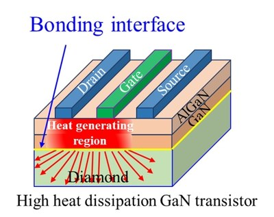
金刚石基氮化镓:
详情发表于国际学术期刊《ADVANCED MATERIALS》。
正在进行研究以实现金刚石上的 GaN 结构。
常规方法:
在传统方法中,在GaN和金刚石之间插入中间层。
因此,散热受阻,
金刚石结晶度不足等。
金刚石的性能没有得到充分发挥,
据说存在上述问题。
这种方法:
旨在解决此类问题,
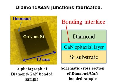
积累在硅衬底上,
在厚度约为 1 μm 的 GaN 薄层表面,
使用金刚石基材和表面活化结合方法。
这样,据说室温下的直接耦合是成功的。
常温直接耦合结果:
去除硅衬底后
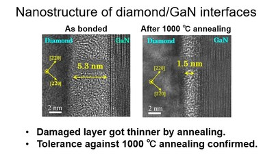
在氮气氛中热处理 GaN 薄层/金刚石。
确认通过高达 1000°C 的热处理保持结合。
调查热处理前后GaN/金刚石键合界面的相关性。
1000℃热处理后
即使晶体在热处理前破碎
确认面积正在减少。
基于此成就:
研究组发现,结合界面可以承受1000℃的热处理。
金刚石结合的 GaN 层经过处理以最大限度地提高金刚石的热导率。
技术+
https://news.mynavi.jp/article/20210910-1969716/
GaN-on-diamond semiconductor material that can take the heat – 1,000℃ to be exact
Summary
Researchers
succeed in the direct bonding of diamond and gallium nitride (GaN) at room temperature and demonstrate that
the bond can withstand heat treatments of 1,000℃, making it ideal for the high temperature fabrication process of GaN-based devices.
GaN-on-diamond semiconductor material will allow for the next generation of high power, high frequency devices.
Research outline
The need for more powerful electronic devices in today’s society
is curtailed by our ability to produce highly conductive semiconductors that can withstand the harsh, high temperature fabrication processes of high-powered devices.
Gallium nitride (GaN)-on-diamond
shows promise as a next-generation semiconductor material due to the wide band gap of both materials, allowing for high conductivity, and diamond’s high thermal conductivity, positioning it as a superior heat-spreading substrate.
There have been attempts at creating a GaN-on-diamond structure by combining the two components with some form of transition or adhesion layer,
but in both cases the additional layer significantly interfered with diamond’s thermal conductivity – defeating a key advantage of the GaN-diamond combination.
There is thus a need for a technology that can directly integrate diamond and GaN,” states Jianbo Liang, Associate Professor of the Graduate School of Engineering, Osaka City University (OCU),
and first author of the study, “However, due to large differences in their crystal structures and lattice constants, direct diamond growth on GaN and vice versa is impossible.”
As reported this week in the journal ADVANCED MATERIALS,
Liang, Shigekawa and their colleagues from Tohoku University,
Saga University,
and Adamant Namiki Precision Jewel. Co., Ltd,use the SAB method to successfully bond GaN and diamond, and demonstrate that the bonding is stable even when heated to 1,000℃.
SAB creates highly strong bonds between different materials at room temperature
by atomically cleaning and activating the bonding surfaces to react when brought into contact with each other.
Osaka City University