
NEDO: World’s First Single-Crystal Diamond from Gas-Next Generation Power Semiconductor Tech
-Realizing a rapid energy saving by developing diamond semiconductors-
March 20, 2019
New Energy Development Organization
National Institute of Advanced Industrial Science and Technology
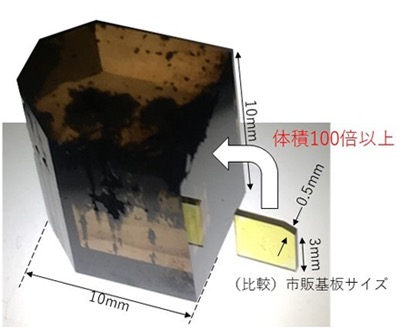
For the first time in the world, we have succeeded in producing single crystal diamond with a volume of 1 cubic centimeter without cracks from gas.
This achievement is a major step in the realization of large wafers.
In the future, we will accelerate the development of next-generation power semiconductors using diamond.
Power semiconductor:
It is an important device that is applied to various facilities and equipment such as electric power infrastructures, automobiles, railway vehicles, industrial equipment and home appliances, and supports their high performance and energy saving.
Instead of silicon (Si) from 2014
- Silicon carbide (SiC)
- Gallium Nitride (GaN)
- Gallium oxide (Ga2O3)
- diamond
We have been promoting technology development to commercialize power semiconductors, and aimed for the highly efficient and compact electric equipment.
Among them, diamond has the highest physical properties such as withstand voltage and thermal conductivity among semiconductor materials.
Results of AIST:
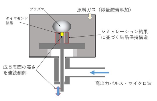
The world’s first microwave plasma CVD method * 4 succeeded in producing a single crystal diamond with a volume of 1 cubic centimeter without cracks from gas.
A method that uses as its raw material gas that can be easily scaled up in synthetic area
By manufacturing the world’s largest crystal, inch-size and large-sized wafers can be realized.
In addition, diamond can handle high spatial resolution quantum information at room temperature and pressure.
- Electronics field such as power semiconductors,
- Spintronics * Application to 5 fields,
- High performance sensor and quantum computing
March 28th, 2019, co-sponsored by Cabinet Office and NEDO
Results report and sample display at the SIP “Next Generation Power Electronics” Open Symposium.