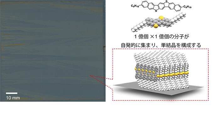
AIST: 10nm ultra-thin organic semiconductor single crystal film wafer: by simple printing method
The Univ of Tokyo / Material Innovation Center / National Institute for Materials Science / Pi-Crystal
The joint research group produced an organic semiconductor wafer that can be used as a high-performance transistor by a simple printing method.
Announcement points:
Succeeded in producing ultra-thin organic semiconductor single-crystal wafers with a thickness of only 10 nanometers using a simple printing method.
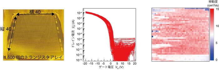
1,600 transistors fabricated on a wafer are all driven without defects
The average mobility is found to be about 10 cm2 / Vs, which is an index for practical use
With the increased printing scale, “mass production of high-speed organic transistor integrated circuits” is expected.
Compared to conventional organic semiconductor printing, this printing method consumes very little material.
In addition, it is thought that process time will be shortened when the printing area is enlarged.
In future industrial applications, significant cost reductions are expected.
The results of this research will be published in the November 4, 2019 edition of the British scientific journal “Scientific Reports“.
https://www.aist.go.jp/aist_j/press_release/pr2019/pr20191105/pr20191105.html