Tohoku University: Mass production of high-quality GaN single crystal substrates:
-Development of low-pressure acidic amonothermal method-
Improved power conversion efficiency:
In order to realize a sustainable society, “improving power conversion efficiency” is an urgent issue.
The solution:
The notable solution is
It is to replace “high frequency power transistor responsible for power control” from silicon to GaN.
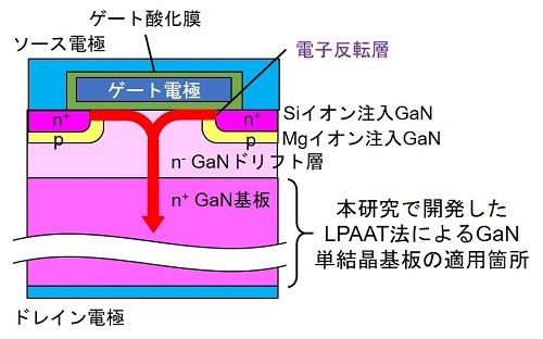
Fabrication of high quality GaN single crystal substrate:
status quo,
It is difficult to “obtain a high-quality GaN single crystal substrate that forms the basis of high-performance GaN transistors.”
“Manufacturing a highly reliable GaN transistor with low leakage current” is extremely difficult.
Tohoku University Institute of Multidisciplinary Materials Science
Professor Shigefusa Chichibu
Collaboratively developed with Tohoku University, Japan Steel Works, and Mitsubishi Chemical.
There is almost no warp,
Large diameter and high purity,
Mass production of GaN single crystal substrates
We have succeeded in developing the “low pressure acidic amonothermal method”.
Science magazine
Applied Physics Express
It was released online on April 17, 2020.
Announcement points
Developed “Crystal fabrication method that can mass-produce gallium nitride * 1 single crystal substrates of 2 inches or more”
Almost no warpage (radius of curvature about 1.5 km)
Crystallinity with very little mosaic,
Excitons * 2 emit light,
Fabrication of high-purity gallium nitride single crystal substrate
Contributing to next-generation power electronics by supplying high-quality gallium nitride substrates
Press Release / Research Results Tohoku University
https://www.tohoku.ac.jp/japanese/2020/06/press20200601-01-GaN.html
Tohoku University: Significance of successful production of “high quality GaN single crystal” (New Switch)
https://news.yahoo.co.jp/articles/a56bac3c841f9b1dbd3436d863c1d574fb1b02f0
Université du Tohoku : Production en série de substrats monocristallins GaN de haute qualité :
-Développement de la méthode amonothermique acide basse pression-
Amélioration de l’efficacité de la conversion de puissance :
Afin de réaliser une société durable, “l’amélioration de l’efficacité de la conversion de l’énergie” est une question urgente.
La solution:
La solution notable est
Il s’agit de remplacer le “transistor de puissance haute fréquence responsable du contrôle de puissance” du silicium par le GaN.
Fabrication d’un substrat monocristallin de GaN de haute qualité :
Status Quo,
Il est difficile “d’obtenir un substrat monocristallin GaN de haute qualité qui constitue la base des transistors GaN hautes performances”.
“Fabriquer un transistor GaN hautement fiable avec un faible courant de fuite” est extrêmement difficile.
Institut universitaire de science des matériaux multidisciplinaire de Tohoku
Professeur Shigefusa Chichibu
Développé en collaboration avec l’Université de Tohoku, Japan Steel Works et Mitsubishi Chemical.
Il n’y a presque pas de déformation,
Grand diamètre et grande pureté,
Production en série de substrats monocristallins GaN
Nous avons réussi à mettre au point la “méthode amonothermique acide à basse pression”.
Revue scientifique
Physique Appliquée Express
Il a été mis en ligne le 17 avril 2020.
Points d’annonce
Développé “Méthode de fabrication de cristaux pouvant produire en masse du nitrure de gallium * 1 substrats monocristallins de 2 pouces ou plus”
Quasiment pas de gauchissement (rayon de courbure d’environ 1,5 km)
Cristallinité avec très peu de mosaïque,
Les excitons * 2 émettent de la lumière,
Fabrication d’un substrat monocristallin de nitrure de gallium de haute pureté
Contribuer à l’électronique de puissance de nouvelle génération en fournissant des substrats de nitrure de gallium de haute qualité
Communiqué de presse / Résultats de recherche Université du Tohoku
Université du Tohoku : importance d’une production réussie de “monocristal de GaN de haute qualité” (nouveau commutateur)
Universität Tohoku: Massenproduktion hochwertiger GaN-Einkristallsubstrate:
-Entwicklung des sauren amonothermalen Niederdruckverfahrens-
Verbesserte Leistungsumwandlungseffizienz:
Um eine nachhaltige Gesellschaft zu verwirklichen, ist die “Verbesserung der Leistungsumwandlungseffizienz” ein dringendes Problem.
Die Lösung:
Die bemerkenswerte Lösung ist
Es soll den “für die Leistungssteuerung verantwortlichen Hochfrequenz-Leistungstransistor” von Silizium durch GaN ersetzen.
Herstellung von hochwertigem GaN-Einkristallsubstrat:
Status Quo,
Es ist schwierig, „ein qualitativ hochwertiges GaN-Einkristallsubstrat zu erhalten, das die Grundlage für Hochleistungs-GaN-Transistoren bildet“.
„Die Herstellung eines hochzuverlässigen GaN-Transistors mit niedrigem Leckstrom“ ist äußerst schwierig.
Institut für multidisziplinäre Materialwissenschaften der Universität Tohoku
Professor Shigefusa Chichibu
In Zusammenarbeit mit der Universität Tohoku, Japan Steel Works und Mitsubishi Chemical entwickelt.
Es gibt fast keine Verzerrung,
Großer Durchmesser und hohe Reinheit,
Massenproduktion von GaN-Einkristallsubstraten
Es ist uns gelungen, das “niederdrucksaure amonothermale Verfahren” zu entwickeln.
Magazin Wissenschaft
Angewandte Physik Express
Es wurde am 17. April 2020 online veröffentlicht.
Ankündigungspunkte
Entwicklung eines „Kristallherstellungsverfahrens, mit dem Galliumnitrid * 1-Einkristallsubstrate von 2 Zoll oder mehr in Massenproduktion hergestellt werden können“
Nahezu kein Verzug (Krümmungsradius ca. 1,5 km)
Kristallinität mit sehr wenig Mosaik,
Exzitonen * 2 emittieren Licht,
Herstellung von hochreinem Galliumnitrid-Einkristallsubstrat
Beitrag zur Leistungselektronik der nächsten Generation durch die Lieferung hochwertiger Galliumnitrid-Substrate
Pressemitteilung / Forschungsergebnisse Universität Tohoku
Universität Tohoku: Bedeutung der erfolgreichen Produktion von „high quality GaN single crystal“ (New Switch)
Ammonothermal growth of 2 inch long GaN single crystals using an acidic NH4F mineralizer in a Ag-lined autoclave
– IOPscience
Abstract
Seeded ammonothermal growths of a few-mm-thick GaN crystals on a 2 inch diameter c-plane and a 45 mm longm-plane GaN wafers
were carried out by using an NH4F mineralizer in a 60 mm diameter Ag-lined autoclave.
As a result of dynamic control of the temperature profile,
low dislocation density and nearly bowing-free m-plane GaN was grown:
i.e. the full-width at half-maximum values for the X-ray rocking curves of the 10$\bar{1}$0 and 10$\bar{1}$ 2 reflections
were smaller than 28 arcsec and the radius of curvature was estimated to be 1460 m.
In addition,
its low temperature photoluminescence spectrum exhibited free and neutral donor-bound exciton emission peaks.
https://iopscience.iop.org/article/10.35848/1882-0786/ab8722