産総研:日台が連携、2nm世代に向け:「hCFET」開発(動画):
AIST: Japan-Taiwan collaborate, for 2nm generation: “hCFET” development:
AIST:日本与台湾合作,开发2nm芯片:“ hCFET”开发
ー200℃以下でSi層とGe層を積層ー
ー大幅な集積化と高速化を可能にー
産総研:日台が連携
2nm世代に向けた積層型Si/Ge異種チャネル相補型電界効果トランジスタhCFETを開発
産業技術総合研究所(産総研)
台湾半導体研究中心(TSRI)日本と台湾の国際共同研究グループ:
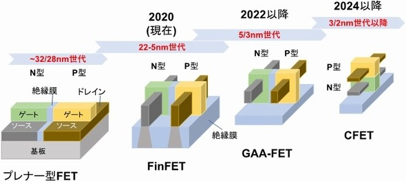
2020年12月、「2nm世代に向け、積層型Si/Ge異種チャネル相補型・電界効果トランジスタ」を、開発したと発表した。
hCFETとは:
heterogeneous Complementary-Field Effect Transistor
日本・産総研:
「Siのn型FETとGeのp型FETを混載したCMOS技術の研究開発」を行ってきた。
台湾・TSRI:
「2nm世代以降の3次元チャネル実現に向け、微細プロセス技術の開発」に取り組んできた。
共同研究プロジェクト:
そこで両者は、それぞれの強みを生かすため国際共同研究プロジェクトを2018年に立ち上げた。
LT-HBTを開発:低温異種材料接合技術
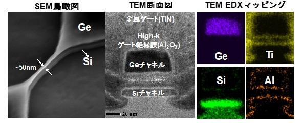
同プロジェクトでは、Si層とGe層を積層したSi/Ge異種チャネル集積プラットフォームを開発した。
- 200℃以下で、
- 高品質のSi層とGe層を積層できる、
- 低温異種材料接合技術(LT-HBT:Low Temperature Hetero-layer Bonding Technology)
を開発した。
LT-HBTの特徴:
- 積層とエッチングのプロセスを、全て低温で行える。
- Si層やGe層に対するダメージが、極めて少ない。
- 高品質のSi/Ge異種チャネル集積プラットフォームを実現できる。
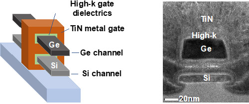
hCFETを作製
研究グループは、開発したSi/Ge異種チャネル積層プラットフォームを用いて、hCFETを作製した。
SiとGe層を
- 同一のチャネルパターンで形成し、
- Si層とGe層の間の絶縁層を取り除くことで、
- ナノシート状の積層型チャネル構造とした。
SEM鳥瞰図により、GeとSiチャネルが露出しているのを確認した。
国際共同研究グループ:
精度の高い異種チャネル集積プラットフォームの確立を急ぐ。
海外を含む民間企業に対して、3年後をめどに技術移転を行う予定である。
EE Times Japan
https://eetimes.jp/ee/articles/2012/09/news044.html
Development of New Transistor Architecture for the 2nm Node Points
Realization of Si/Ge heterogeneous channel platform for the 2nm node through international collaboration between Japan and Taiwan semiconductor research institutes
Development of new transistor architecture consisting of vertically stacked Si nFET/Ge pFET
Contribution to high speed and low power consumption of very large scaled integrated circuits
Background
Owing to the explosive spread of IT devices, there is a huge demand for high performance and low power consumption of integrated circuits.
Ge possess higher hole mobility than that of Si and can operate under lower gate voltage.
Therefore, the CMOS technology composing of a Si nFET and a Ge pFET
is strongly needed.In 2001, AIST started the research on high performance Ge transistors.
On the other hand, the development of 3-dimensional ultra-scaled process technology for beyond the 2nm node has strongly been pushed by the Taiwan Semiconductor Research Institute (TSRI), Taiwan.
In 2018, the international collaboration between AIST and TSRI started.
https://www.aist.go.jp/aist_e/list/latest_research/2020/20201208/en20201208.html