AIST: Japan-Taiwan collaborate, for 2nm generation: “hCFET” development
-Laminate Si layer and Ge layer at 200 ° C or less-
-Achieves significant integration and speed-
AIST: Japan and Taiwan collaborate
Developed stacked Si / Ge heterogeneous channel complementary field effect transistor hCFET for 2nm generation
National Institute of Advanced Industrial Science and Technology (AIST)
Taiwan Semiconductor Research Center (TSRI)
International Joint Research Group of Japan and Taiwan:
In December 2020, it announced that it had developed a “stacked Si / Ge heterogeneous channel complementary type field effect transistor for the 2nm generation.”
What is hCFET:
heterogeneous Complementary-Field Effect Transistor
Japan AIST:
We have been conducting “Research and development of CMOS technology in which Si n-type FET and Ge p-type FET are mixedly mounted”.
Taiwan / TSRI:
We have been working on “development of fine process technology for the realization of 3D channels after the 2nm generation”.
Joint research project:
Therefore, both sides launched an international joint research project in 2018 to utilize their respective strengths.
Developed LT-HBT: Low temperature dissimilar material joining technology
In this project, we have developed a Si / Ge heterogeneous channel integration platform in which Si and Ge layers are stacked.
At 200 ° C or below
High quality Si layer and Ge layer can be laminated,
Low Temperature Hetero-layer Bonding Technology (LT-HBT)
Was developed.
Features of LT-HBT:
The laminating and etching processes can all be done at low temperatures.
Very little damage to the Si and Ge layers.
A high quality Si / Ge heterogeneous channel integration platform can be realized.
Manufacture hCFET
The research group created hCFETs using the developed Si / Ge heterogeneous channel stacking platform.
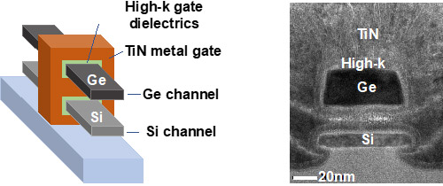
Si and Ge layers
Formed with the same channel pattern,
By removing the insulating layer between the Si layer and the Ge layer
It has a nanosheet-like laminated channel structure.
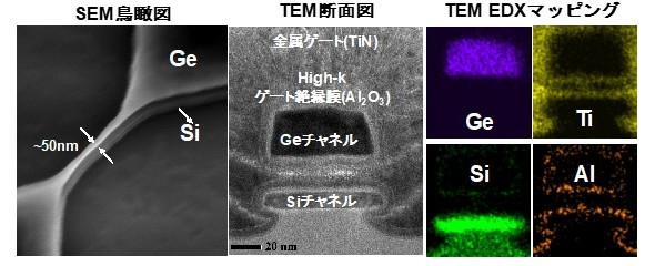
A bird’s-eye view of SEM confirmed that the Ge and Si channels were exposed.
International Collaborative Research Group:
We will hurry to establish a highly accurate heterogeneous channel integration platform.
Against private companies, including overseas, it is expected to carry out the technology transfer to the prospect of three years.
EE Times Japan
https://eetimes.jp/ee/articles/2012/09/news044.html
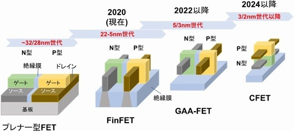
Development of New Transistor Architecture for the 2nm Node Points
Realization of Si/Ge heterogeneous channel platform for the 2nm node through international collaboration between Japan and Taiwan semiconductor research institutes
Development of new transistor architecture consisting of vertically stacked Si nFET/Ge pFET
Contribution to high speed and low power consumption of very large scaled integrated circuits
Background
Owing to the explosive spread of IT devices, there is a huge demand for high performance and low power consumption of integrated circuits.
Ge possess higher hole mobility than that of Si and can operate under lower gate voltage.
Therefore, the CMOS technology composing of a Si nFET and a Ge pFET
is strongly needed.In 2001, AIST started the research on high performance Ge transistors.
On the other hand, the development of 3-dimensional ultra-scaled process technology for beyond the 2nm node has strongly been pushed by the Taiwan Semiconductor Research Institute (TSRI), Taiwan.
In 2018, the international collaboration between AIST and TSRI started.
https://www.aist.go.jp/aist_e/list/latest_research/2020/20201208/en20201208.html