AIST:日本与台湾合作,开发2nm芯片:“ hCFET”开发
-在200°C或更低的温度下层压硅层和锗层-
-实现显着的集成和速度-
AIST:日本和台湾合作
开发用于2nm世代的堆叠式Si / Ge异质沟道互补电场效应晶体管hCFET
工业技术研究院(AIST)
台积电研究中心(TSRI)
日本和台湾国际联合研究小组:
2020年12月,它宣布已开发出“用于2nm世代的多层Si / Ge异质沟道互补电场效应晶体管”。
什么是hCFET:
异质互补场效应晶体管
日本AIST:
我们一直在进行“将Si n型FET和Ge p型FET混合安装的CMOS技术的研究与开发”。
台湾/ TSRI:
我们一直在致力于“开发精细工艺技术,以在2nm世代之后实现3D通道”。
联合研究项目:
因此,双方于2018年启动了一项国际联合研究项目,以利用各自的优势。
开发LT-HBT:低温异种材料接合技术
在此项目中,我们开发了一个Si / Ge异质通道集成平台,其中堆叠了Si和Ge层。
200°C以下
可以层叠高质量的Si层和Ge层,
低温异质层键合技术(LT-HBT)
已开发。
LT-HBT的特点:
层压和蚀刻工艺都可以在低温下完成。
对Si和Ge层的损害很小。
可以实现高质量的Si / Ge异质通道集成平台。
制造hCFET
该研究小组使用已开发的Si / Ge异质通道堆叠平台创建了hCFET。
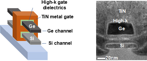
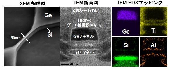
硅和锗层
以相同的渠道模式形成
通过去除Si层和Ge层之间的绝缘层
使用了纳米片状的层压通道结构。
SEM的鸟瞰图证实了Ge和Si通道已暴露。
国际合作研究小组:
我们将尽快建立一个高度准确的异构渠道集成平台。
对于包括海外的私人公司,预计将进行为期三年的技术转让。
EE Times日本
https://eetimes.jp/ee/articles/2012/09/news044.html
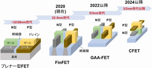
Development of New Transistor Architecture for the 2nm Node Points
Realization of Si/Ge heterogeneous channel platform for the 2nm node through international collaboration between Japan and Taiwan semiconductor research institutes
Development of new transistor architecture consisting of vertically stacked Si nFET/Ge pFET
Contribution to high speed and low power consumption of very large scaled integrated circuits
Background
Owing to the explosive spread of IT devices, there is a huge demand for high performance and low power consumption of integrated circuits.
Ge possess higher hole mobility than that of Si and can operate under lower gate voltage.
Therefore, the CMOS technology composing of a Si nFET and a Ge pFET
is strongly needed.In 2001, AIST started the research on high performance Ge transistors.
On the other hand, the development of 3-dimensional ultra-scaled process technology for beyond the 2nm node has strongly been pushed by the Taiwan Semiconductor Research Institute (TSRI), Taiwan.
In 2018, the international collaboration between AIST and TSRI started.
https://www.aist.go.jp/aist_e/list/latest_research/2020/20201208/en20201208.html