キヤノンのNIL:EUVより低コストで微細化
Canon’s NIL: Miniaturization at a lower cost than EUV
佳能的NIL:比EUV成本更低的小型化
・NILを、米テキサス大・TIEに提供開始
・ナノインプリントリソグラフィは、低価格で半導体を製造可能
ニュースイッチ掲載記事からSummaryをお届けします。
キヤノンのNIL:
キヤノンの次世代半導体製造装置・ナノインプリントリソグラフィ(NIL)が動き出す。
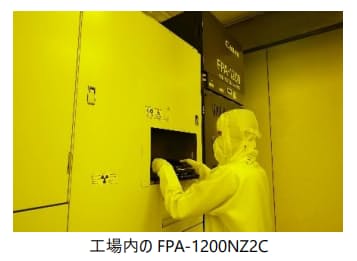
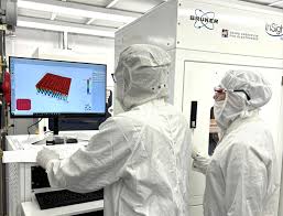
キヤノンは9月26日、NIL装置を発売後初めて納入すると発表した。

米テキサス大学:オースティン校:
半導体研究のコンソーシアム「TIE」向けに、出荷を開始した。
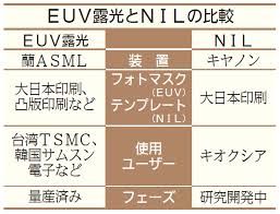
1.先端半導体製造では、蘭ASMLのEUV露光装置が覇権を握る。
2.キヤノンは、NIL装置を投入し、最先端露光装置への参入を狙う。
今回納入するNILは、TIEで半導体デバイス試作に使われる。

先端半導体回路の微細化:
「NILは低価格で先端半導体を製造でき、試作に向く」と話す。
NILは、先端半導体分野参入の「戦略装置」だ。
ASMLの露光装置は、回路微細化が進むごとに、波長の短い光源を使う。
1.特に7nm以下の先端半導体では、EUV露光装置が不可欠だ。
2.一方、光源の波長が短くなると、物質に吸収されやすくなる。
ASMLのEUV露光装置:
EUVは、光源の出力を高めることで、先端半導体を実現する。
ただし、EUV露光装置の製造は極めて難しく、ASMLが独占中。
ニコンとキヤノンは厳しい開発競争で、ASMLに敗れた。
現在ASMLが、世界で唯一製造する。
キャノンのNIL装置開発:
キヤノンは、10年ぶりに最先端露光装置への参入を目指す。
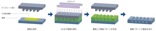
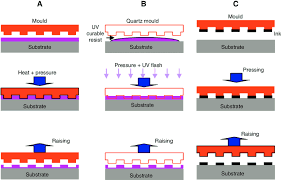
1.NILは、従来の光を転写する露光装置ではない。
2.NILは、はんこを押すように、回路を形成できる。
NIL装置は、EUV装置に比べ、簡便な方法で微細回路を形成する。
キヤノンのNIL開発プロセス:
2014年、キヤノンは、米モレキュラーインプリントを買収した。
キャノンは3社で共同開発:
1.キャノンは、一号機をキオクシアに同装置を納入。
2.キヤノン、キオクシア、大日本印刷の3社で共同開発した。
2023年発売を開始、実用化まで10年を投じてきた。
岩本副事業本部長の指摘:
NIL普及のカギは、先端半導体・量産ラインでの利用を推進することだ。
1.EUV装置はコストが高い、利用頻度削減がメーカーの課題だ。
2.NIL装置は、消費電力が少なく、コストダウンに貢献する。
今後、フォトマスクのサプライチェーンの構築を進める。
3―5年後、年間十数台の販売を目指す。
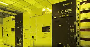
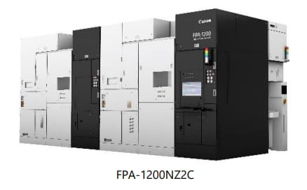
Canon delivers FPA -1200NZ2C nanoimprint lithography system
for semiconductor manufacturing to the Texas Institute for Electronics
From Canon Global report
TOKYO, September 26, 2024—
Canon Inc. announced today:
Canon will ship its most advanced lithography platform,
the FPA-1200NZ2C nanoimprint lithography (NIL) system for semiconductor manufacturing,
to the Texas Institute for Electronics (TIE), a Texas-based semiconductor consortium, on September 26, 2024.

Canon’s NIL technology:
Canon became the first in the world to commercialize a semiconductor manufacturing system that uses NIL technology,
which forms circuit patterns in a different method from conventional projection exposure technology, when it released the FPA-1200NZ2C on October 13, 2023.
NIL photolithography equipment:
In contrast to conventional photolithography equipment which transfers a circuit pattern by projecting it onto the resist coated wafer,
the new product does it by pressing a mask imprinted with the circuit pattern into the resist on the wafer like a stamp.
Because its circuit pattern transfer process does not go through an optical mechanism, fine circuit patterns on the mask can be faithfully reproduced on the wafer.
With reduced power consumption and cost :
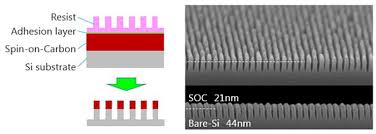
the new system enables patterning with a minimum linewidth of 14 nm1, equivalent to the 5 nm node2 that is required to produce most advanced logic semiconductors currently available.
TIE is a semiconductor consortium:
This FPA-1200NZ2C will be used at TIE for the research and development of advanced semiconductors and production of prototypes.
TIE is a semiconductor consortium which was founded in 2021 and is supported by The University of Texas at Austin.
It consists of state and local governments, semiconductor companies, national research institutions and other entities.
TIE provides open access to semiconductor research and development initiatives and prototyping facilities in order to help solve issues related to advanced semiconductor technology, including advanced packaging technology.
Canon will continue to promote research and development using nanoimprint lithography systems for semiconductor manufacturing to contribute to the evolution of semiconductor manufacturing technology.
https://global.canon/en/news/2024/20240926.html