佳能的NIL:比EUV成本更低的小型化
Canon’s NIL:
Canon’s next-generation semiconductor manufacturing equipment, nanoimprint lithography (NIL), is on the move.
On September 26, Canon announced that it will deliver its first NIL equipment since its release.

University of Texas at Austin:
Shipments have begun to the semiconductor research consortium TIE.
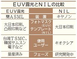
1. Dutch ASML’s EUV exposure equipment dominates advanced semiconductor manufacturing.
2. Canon aims to enter the cutting-edge exposure equipment market by introducing NIL equipment.
The NIL delivered this time will be used at TIE to prototype semiconductor devices.

Miniaturization of advanced semiconductor circuits:
“NIL can manufacture advanced semiconductors at low cost, and is suitable for prototyping,” he says.
NIL is a “strategic device” for entering the advanced semiconductor field.
ASML’s exposure equipment uses light sources with shorter wavelengths as circuits become finer.
1. EUV exposure equipment is essential, especially for advanced semiconductors below 7 nm.
2. On the other hand, as the wavelength of the light source becomes shorter, it becomes more easily absorbed by materials.
ASML’s EUV exposure equipment:
EUV realizes advanced semiconductors by increasing the output of the light source.
However, EUV exposure equipment is extremely difficult to manufacture, and ASML has a monopoly on it.
Nikon and Canon lost to ASML in a fierce development race.
Currently, ASML is the only company in the world that manufactures it.
Canon’s development of NIL equipment:
Canon aims to enter the cutting-edge exposure equipment market for the first time in 10 years.
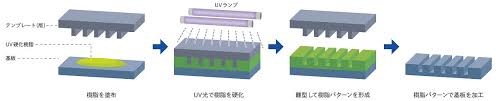
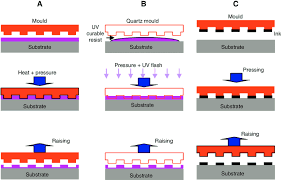
1. NIL is not a conventional exposure equipment that transfers light.
2. NIL can form circuits as if stamping a stamp.
Compared to EUV equipment, NIL equipment forms fine circuits in a simpler way.
Canon’s NIL development process:
In 2014, Canon acquired Molecular Imprints, a US company.
Canon jointly developed with three companies:
1. Canon delivered the first machine to Kioxia.
2. Canon, Kioxia, and Dai Nippon Printing jointly developed the device.
It was launched in 2023, and 10 years were spent until it was put into practical use.
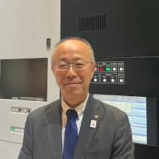
Iwamoto, Deputy General Manager of the Business Unit, points out:
The key to the spread of NIL is to promote its use in advanced semiconductor and mass production lines.
1. EUV equipment is expensive, and manufacturers need to reduce the frequency of use.
2. NIL equipment consumes little power, which contributes to cost reduction.
We will continue to build a supply chain for photomasks in the future.
The goal is to sell a dozen units per year in the next three to five years.
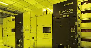
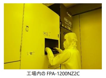
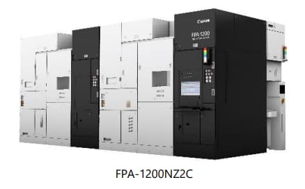
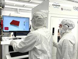
Canon delivers FPA -1200NZ2C nanoimprint lithography system
for semiconductor manufacturing to the Texas Institute for Electronics
From Canon Global report
TOKYO, September 26, 2024—
Canon Inc. announced today:
Canon will ship its most advanced lithography platform,
the FPA-1200NZ2C nanoimprint lithography (NIL) system for semiconductor manufacturing,
to the Texas Institute for Electronics (TIE), a Texas-based semiconductor consortium, on September 26, 2024.

Canon’s NIL technology:
Canon became the first in the world to commercialize a semiconductor manufacturing system that uses NIL technology,
which forms circuit patterns in a different method from conventional projection exposure technology, when it released the FPA-1200NZ2C on October 13, 2023.
NIL photolithography equipment:
In contrast to conventional photolithography equipment which transfers a circuit pattern by projecting it onto the resist coated wafer,
the new product does it by pressing a mask imprinted with the circuit pattern into the resist on the wafer like a stamp.
Because its circuit pattern transfer process does not go through an optical mechanism, fine circuit patterns on the mask can be faithfully reproduced on the wafer.
With reduced power consumption and cost :
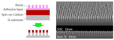
the new system enables patterning with a minimum linewidth of 14 nm1, equivalent to the 5 nm node2 that is required to produce most advanced logic semiconductors currently available.
TIE is a semiconductor consortium:
This FPA-1200NZ2C will be used at TIE for the research and development of advanced semiconductors and production of prototypes.
TIE is a semiconductor consortium which was founded in 2021 and is supported by The University of Texas at Austin.
It consists of state and local governments, semiconductor companies, national research institutions and other entities.
TIE provides open access to semiconductor research and development initiatives and prototyping facilities in order to help solve issues related to advanced semiconductor technology, including advanced packaging technology.
Canon will continue to promote research and development using nanoimprint lithography systems for semiconductor manufacturing to contribute to the evolution of semiconductor manufacturing technology.
https://global.canon/en/news/2024/20240926.html