レーザーテック:半導体ウエハーを15分で全面検査(動画):
Lasertec: Full inspection of semiconductor wafers in 15 minutes:
Lasertec:在 15 分钟内对半导体晶片进行全面检测:
ー「OPTELICS AI²」で製品化ー
レーザーテック:
- 追従式自動焦点(AF)の連続走査により、
- 3インチウエハーを15分で全面検査する、
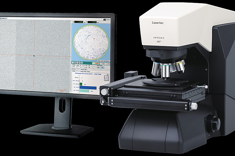
コンフォーカル顕微鏡自動検査/レビュー装置を製品化した。
「OPTELICS AI²」:
- 半導体ウエハーのほか、
- フィルム、ガラス基板など、
「自動検査から、欠陥の分類・解析、3D形状測定」まで1台で対応する。
販売価格:
価格は、仕様により消費税抜きで、5000万円から販売。
歩留まり向上に貢献:
- 研究開発部門にとどまらず、
- 量産試作品の評価、
- 歩留まり向上に向けたプロセス改善など、
半導体デバイス開発のスピードアップに貢献する。
高倍率形状測定を両立:
半導体検査装置で培ってきたソフト技術に、高性能マイコンを組み合わせた。
「高速検査機能」と「高コントラストのコンフォーカル光学系による高倍率形状測定」を両立した。
追従式AFの採用:
追従式AFにより、
- 化合物半導体やガラス基板など、
- 透明な試料でも裏面反射に影響されずに検査・測定。
自動検査AIソフト:
自動検査ソフトには、
「ディープラーニングに基づく、人工知能(AI)機能」を組み込んだ。
ニュースイッチ
New product release: OPTELICS AI² Automatic Inspection and Review System
Lasertec Corporation
Automatic defect inspection, high-magnification review, and 3D surface shape profiling all in a single device.
Lasertec Corporation today announced the release of OPTELICS AI2,
a confocal microscope-based automatic inspection and review system.
Detail Description Lasertec has launched OPTELICS AI2,
a new type of confocal microscope designed to perform automatic defect inspection and review.
AI2 provides
high-speed automatic surface defect inspection, defect mapping, and high-magnification defect shape review from a single platform.There has been a rapid increase in demand for semiconductor devices due to growing need for
5G mobile communication,
high-performance computing,
and other applications.Semiconductor device manufacturers are expected to keep developing new devices with increased performance.
For the development of new devices adopting new designs and new materials,
various challenges need to be overcome with cross-organizational efforts.
The evaluation of prototypes, quality control during production, and process improvement
for higher yields are among those challenges.
AI2 performs
automatic surface defect inspection, defect review,
and defect shape 3D profiling on a single platform,
serving customer need in various situations of R&D and production.AI2 achieves
both high-throughput, high-speed inspection and high-magnification surface shape profiling
by integrating Lasertec’s core technology in confocal optics,automatic inspection software perfected through the development of various semiconductor-related inspection systems,
and newly designed high-speed motion hardware into a system.
AI2 conducts AI-based inspection
using deep learning and offers advanced inspection functions such as high-precision image classification,patterned sample inspection, and the extraction of specific types of defects.
Lasertec is dedicated to addressing customer need and helping customers succeed in various R&D and yield improvement efforts.