Lasertec:在 15 分钟内对半导体晶片进行全面检测:
-与“OPTELICS AI²”一起商业化-
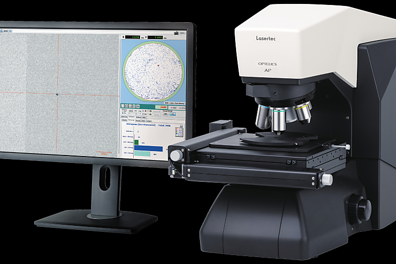
激光技术:
连续扫描后续自动对焦(AF)
3英寸晶圆15分钟全检,
商业化共聚焦显微镜自动检查/审查设备。
“光学AI²”:
除了半导体晶圆
薄膜、玻璃基板等
一台设备可以处理从自动检查到缺陷分类/分析和 3D 形状测量的所有事情。
售价:
价格从 5000 万日元起,不含消费税,具体取决于规格。
有助于提高产量:
不限于研发部门
评估批量生产原型,
工艺改进以提高产量等。
有助于加快半导体器件的发展。
两种高倍形状测量:
高性能微型计算机与在半导体检测设备中培养的软件技术相结合。
实现了“高速检查功能”和“高对比度共焦光学系统的高倍率形状测量”。
采用后续AF:
有后续AF
化合物半导体、玻璃基板等
不受背面反射影响的透明样品的检查和测量。
自动检测AI软件:
对于自动检测软件,
加入“基于深度学习的人工智能(AI)功能”。
新开关
New product release: OPTELICS AI² Automatic Inspection and Review System
Lasertec Corporation
Automatic defect inspection, high-magnification review, and 3D surface shape profiling all in a single device.
Lasertec Corporation today announced the release of OPTELICS AI2,
a confocal microscope-based automatic inspection and review system.
Detail Description Lasertec has launched OPTELICS AI2,
a new type of confocal microscope designed to perform automatic defect inspection and review.
AI2 provides
high-speed automatic surface defect inspection, defect mapping, and high-magnification defect shape review from a single platform.There has been a rapid increase in demand for semiconductor devices due to growing need for
5G mobile communication,
high-performance computing,
and other applications.Semiconductor device manufacturers are expected to keep developing new devices with increased performance.
For the development of new devices adopting new designs and new materials,
various challenges need to be overcome with cross-organizational efforts.
The evaluation of prototypes, quality control during production, and process improvement
for higher yields are among those challenges.
AI2 performs
automatic surface defect inspection, defect review,
and defect shape 3D profiling on a single platform,
serving customer need in various situations of R&D and production.AI2 achieves
both high-throughput, high-speed inspection and high-magnification surface shape profiling
by integrating Lasertec’s core technology in confocal optics,automatic inspection software perfected through the development of various semiconductor-related inspection systems,
and newly designed high-speed motion hardware into a system.
AI2 conducts AI-based inspection
using deep learning and offers advanced inspection functions such as high-precision image classification,patterned sample inspection, and the extraction of specific types of defects.
Lasertec is dedicated to addressing customer need and helping customers succeed in various R&D and yield improvement efforts.