Lasertec: Full inspection of semiconductor wafers in 15 minutes:
-Commercialized with “OPTELICS AI²”-
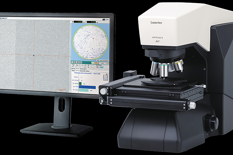
Lasertec:
With continuous scanning of follow-up autofocus (AF)
Full inspection of 3-inch wafer in 15 minutes,
Commercialized a confocal microscope automatic inspection / review device.
“OPTELICS AI²”:
In addition to semiconductor wafers
Film, glass substrate, etc.
One unit can handle everything from automatic inspection to defect classification / analysis and 3D shape measurement.
Selling price:
The price starts from 50 million yen, excluding consumption tax, depending on the specifications.
Contributes to yield improvement:
Not limited to the R & D department
Evaluation of mass production prototypes,
Process improvement to improve yield, etc.
Contributes to speeding up the development of semiconductor devices.
Both high-magnification shape measurement:
A high-performance microcomputer is combined with the software technology cultivated in semiconductor inspection equipment.
Both “high-speed inspection function” and “high-magnification shape measurement with high-contrast confocal optical system” are achieved.
Adoption of follow-up AF:
With follow-up AF
Compound semiconductors, glass substrates, etc.
Inspection and measurement of transparent samples without being affected by backside reflection.
Automatic inspection AI software:
For automatic inspection software,
“Artificial intelligence (AI) function based on deep learning” was incorporated.
New switch
New product release: OPTELICS AI² Automatic Inspection and Review System
Lasertec Corporation
Automatic defect inspection, high-magnification review, and 3D surface shape profiling all in a single device.
Lasertec Corporation today announced the release of OPTELICS AI2,
a confocal microscope-based automatic inspection and review system.
Detail Description Lasertec has launched OPTELICS AI2,
a new type of confocal microscope designed to perform automatic defect inspection and review.
AI2 provides
high-speed automatic surface defect inspection, defect mapping, and high-magnification defect shape review from a single platform.There has been a rapid increase in demand for semiconductor devices due to growing need for
5G mobile communication,
high-performance computing,
and other applications.Semiconductor device manufacturers are expected to keep developing new devices with increased performance.
For the development of new devices adopting new designs and new materials,
various challenges need to be overcome with cross-organizational efforts.
The evaluation of prototypes, quality control during production, and process improvement
for higher yields are among those challenges.
AI2 performs
automatic surface defect inspection, defect review,
and defect shape 3D profiling on a single platform,
serving customer need in various situations of R&D and production.AI2 achieves
both high-throughput, high-speed inspection and high-magnification surface shape profiling
by integrating Lasertec’s core technology in confocal optics,automatic inspection software perfected through the development of various semiconductor-related inspection systems,
and newly designed high-speed motion hardware into a system.
AI2 conducts AI-based inspection
using deep learning and offers advanced inspection functions such as high-precision image classification,patterned sample inspection, and the extraction of specific types of defects.
Lasertec is dedicated to addressing customer need and helping customers succeed in various R&D and yield improvement efforts.