Semiconductor wafers: Detect defects with AI!
– Lasertec improves defect resolution –
– Whole surface inspection of semiconductor wafer in 15 minutes –
Lasertech:
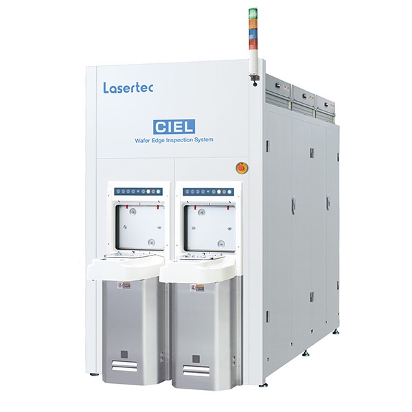
Started accepting orders for the high-sensitivity wafer edge inspection equipment “CIEL Series = Photo”.
CIEL series:
– Improving the yield of semiconductor wafers! ー
Detects “minor edge/edge face defects on semiconductor wafers”.
“We redesigned the optical system of the conventional model to increase the resolution.”
Defects to be detected are identified by deep learning AI.
Price and features:
The series will start with 300mm wafer compatible machines.
Causes of Wafer Defects:
-Miniaturization and high layering of semiconductor processes-
Defect factors that occur on the edge and edge of the wafer are
It is diversified with “in addition to scratches and chips, dust generation and chemical scattering, etc.”
3D shape measurement performance:
CIEL uses high-resolution color images to enhance the ability to measure 3D shapes.
– It is possible to identify minute defects –
It supports each process of semiconductor manufacturing such as exposure, film formation, etching, and cleaning.
new switch
Equipment that inspects the entire surface of a semiconductor wafer in 15 minutes. Commercialized by Lasertec | New Switch
Wafers semi-conducteurs : Détectez les défauts avec l’IA !
– Lasertec améliore la résolution des défauts –
– Inspection de toute la surface d’une tranche de semi-conducteur en 15 minutes –
Lasertech :
A commencé à accepter des commandes pour l’équipement d’inspection des bords de tranches à haute sensibilité “Série CIEL = Photo”.
Série CIEL :
– Améliorer le rendement des plaquettes semi-conductrices ! ー
Détecte les “défauts mineurs de bord/face de bord sur les plaquettes semi-conductrices”.
“Nous avons repensé le système optique du modèle conventionnel pour augmenter la résolution.”
Les défauts à détecter sont identifiés par l’IA d’apprentissage en profondeur.
Prix et fonctionnalités :
La série commencera avec des machines compatibles avec les tranches de 300 mm.
Causes des défauts de plaquette :
-Miniaturisation et superposition de procédés semi-conducteurs-
Les facteurs de défaut qui se produisent sur le bord et le bord de la plaquette sont
Il est diversifié avec “en plus des rayures et des éclats, la génération de poussière et la diffusion de produits chimiques, etc.”
Performances de mesure de forme 3D :
CIEL utilise des images couleur haute résolution pour améliorer la capacité de mesurer des formes 3D.
– Il est possible d’identifier des défauts infimes –
Il prend en charge chaque processus de fabrication de semi-conducteurs tels que l’exposition, la formation de film, la gravure et le nettoyage.
nouvel interrupteur
Équipement qui inspecte toute la surface d’une tranche de semi-conducteur en 15 minutes. Commercialisé par Lasertec | Nouveau commutateur
Halbleiterwafer: Defekte erkennen mit KI!
– Lasertec verbessert Fehlerauflösung –
– Vollständige Oberflächeninspektion von Halbleiterwafern in 15 Minuten –
Lasertechnik:
Beginn der Annahme von Bestellungen für die hochempfindliche Waferkanten-Inspektionsausrüstung “CIEL Series = Photo”.
CIEL-Reihe:
– Verbesserung der Ausbeute an Halbleiterwafern! ー
Erkennt „geringfügige Kanten-/Kantenflächendefekte auf Halbleiterwafern“.
„Wir haben das optische System des konventionellen Modells überarbeitet, um die Auflösung zu erhöhen.“
Zu detektierende Fehler werden durch Deep-Learning-KI identifiziert.
Preis und Ausstattung:
Die Serie beginnt mit 300-mm-Wafer-kompatiblen Maschinen.
Ursachen von Waferdefekten:
-Miniaturisierung und Hochschichtung von Halbleiterprozessen-
Defektfaktoren, die am Rand und am Rand des Wafers auftreten, sind
Es ist diversifiziert mit “zusätzlich zu Kratzern und Spänen, Stauberzeugung und chemischer Streuung usw.”
Leistung der 3D-Formmessung:
CIEL verwendet hochauflösende Farbbilder, um die Fähigkeit zum Messen von 3D-Formen zu verbessern.
– Es ist möglich, kleinste Fehler zu identifizieren –
Es unterstützt jeden Prozess der Halbleiterherstellung wie Belichtung, Filmbildung, Ätzen und Reinigen.
neuer Schalter
Ausrüstung, die die gesamte Oberfläche eines Halbleiterwafers in 15 Minuten inspiziert. Kommerziell von Lasertec | Neuer Schalter
CIEL Series | Lasertec Corporation
Highly accurate classification of wafer edge and bevel defects that are not detectable by existing tools
Topics
2022.12.01
Lasertec releases CIEL Series High Sensitivity Wafer Edge Inspection System
Features Identification of small defects that cannot be detected or classified by existing tools
A high-throughput mode adaptable to meet operational needs 3D profiling capability
Applications
Wafer edge and bevel inspection for process monitoring and feedback in semiconductor device manufacturing processes
Identification of yield-critical defects Process improvement based on 3D measurement
https://www.lasertec.co.jp/en/products/semiconductor/ciel.html