Detects defects automatically Source: Mipox
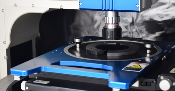
Crystal dislocation high-speed observation device “XS-1 Sirius” Source: Mipox
Mipox: Significantly improved productivity of SiC power semiconductors: Non-destructive and automatic detection of defects
Mipox and Nagoya University:
We jointly developed a “defect identification system that greatly increases the productivity of power semiconductors.”
In semiconductor substrates made of SiC, etc.
Types and positions of missing crystals,
Non-destructive killer defects
Detect automatically.
Difficulties of SiC (Silicon Carbide):
SiC contains crystal loss (dislocation).
In particular, it includes “killer defects” that reduce performance, reliability, and device yield.
As a result, prices remain high, hindering their widespread use.
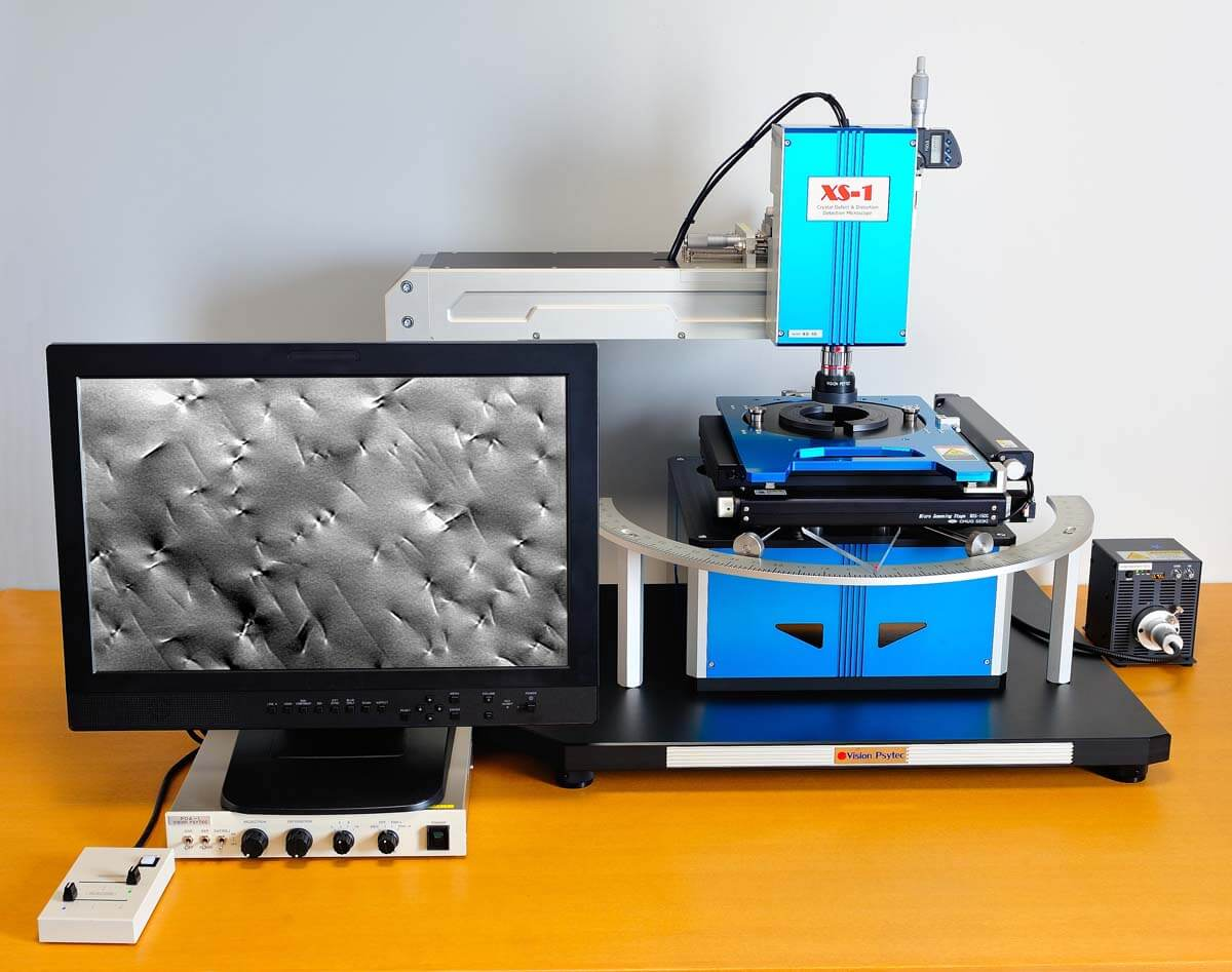
Visualization with birefringence imaging:
In the joint research, we analyzed many dislocations contained in semiconductor substrates such as SiC.
Visualization was performed by “birefringence imaging” to capture the distortion of dislocations.
Simulation and ML (Machine Learning):
Developed a system that automatically detects the type and position of dislocations in a non-destructive manner.
We have developed a system to identify killer defects.
FA News-MONOist
https://monoist.atmarkit.co.jp/mn/articles/2102/05/news025.html
AIST / Nagoya University: Adopts the latest SiC / GaN wafer observation device “XS-1”
Mipox:
Mipox has delivered “XS-1” to AIST / Advanced Power Electronics Research Center and Nagoya University.
SiC crystal dislocation / high-sensitivity visualization device XS-1:
Visualize and observe internal strain due to crystal dislocations inside single crystal SiC / GaN wafers.
Observation of single crystal wafer defects is important:
“SiC / GaN” is attracting a great deal of attention as a new material for next-generation power semiconductors.
Observation of crystal defects contained in single crystal wafers is also important to support the expansion of these markets.
The “XS-1” is equipped with a polarizing optical system that is far more sensitive than conventional polarizing microscopes on the market.
Characteristics of power semiconductor devices and
For the reliability of power semiconductor devices
Derived from crystal dislocations, which can have adverse effects,
“Observation by visualization of crystal internal distortion” is realized.
Research results of AIST:
It was confirmed that the “sensitivity of XS-1 to crystal dislocations of SiC wafers” is “comparable to synchrotron radiation X-ray topography”.
It was also adopted by Nagoya University as a crystal dislocation visualization device for GaN wafers.
What is Mipox:
A manufacturer of abrasives and polishing equipment, and sells optical observation and visualization equipment.
With the innovative XS-1, next-generation power semiconductor materials such as SiC and GaN, and
It is expected that the accuracy and throughput of crystal dislocation observation of sapphire, AlN, diamond, etc. will be dramatically improved.
“XS-1”:
https://product.mipox.co.jp/products/observation/item_30
https://product.mipox.co.jp/product_info/20171201_xs-1.html
Joint research “Development of automatic killer defect inspection system to improve the productivity of semiconductor manufacturing”