“Dynamic AGE-ing” that can replace the conventional mechanical polishing and CMP process
-Can be applied to poor quality SiC wafers (high BPD density)-
Benefits can be obtained even when the epitaxial layer grows Source: Kwansei Gakuin University
Toyota Tsusho: Next-generation power semiconductors, SiC substrate with zero defects: Dynamic AGE-ing®
-Supply samples to device manufacturers aiming for early mass production-
March 01, 2021
Toyota Tsusho:
Kwansei Gakuin University:
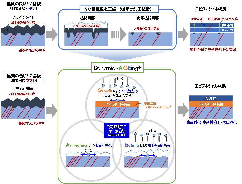
Next-generation power semiconductor material We have developed “Dynamic AGE-ing ®”, a surface nano-control process technology that detoxifies defects * in SiC substrates.
“Dynamic AGE-ing ®”:
This technology is an innovative technology that “realizes high quality and productivity improvement of SiC substrate at the same time”.
We have completed performance verification on a 6-inch SiC board.
Next Generation Power Semiconductor Material SiC Substrate:
SiC substrates are expected to be in great demand in a wide range of fields, including the rapidly electrifying global automobile industry.
It is a material that will contribute to a future decarbonized society.
Started supplying samples to semiconductor manufacturers:
In the future, we will start supplying samples to semiconductor device manufacturers and proceed with evaluation and verification for the introduction of this technology to mass production lines.
We will also accelerate development for application to large-diameter 8-inch SiC substrates, which are expected to become widespread.
Problems with conventional SiC substrates:
“Stable supply of high-quality, large-diameter SiC substrates” is required to “manufacture highly reliable power semiconductors at low cost.”
However, conventional SiC substrates have been
Crystal strain (machining strain layer) generated by machining and
Due to Basal Plane Dislocation (BPD) defects
The issue was that the performance of the power semiconductors formed on it would decline.
Solved by Dynamic AGE-ing®:
The unique technology “Dynamic AGE-ing ®” is different from conventional machining.
A non-contact nano-controlled process technology that integrates thermal etching and crystal growth.
This technology
By placing the SiC substrate in a gas phase environment under ultra-high temperature
Autonomously align the atomic arrangement on the surface,
Achieves complete removal of processing strain layer and detoxification by blocking propagation of BPD (see Chart 1)
By applying “Dynamic AGE-ing ®”, we can improve the quality of SiC substrates regardless of manufacturer or size.
Furthermore, by simplifying the substrate manufacturing process and improving the yield, it is possible to improve the productivity of SiC substrates (see Chart 2).
Press Room | Toyota Tsusho Corporation
https://www.toyota-tsusho.com/press/detail/210301_004770.html
Detoxifying defects in SiC wafers: Innovative process development,
-To reduce the cost of SiC devices-
Green Mobility Material Development Project Project Leader
Mr. Tadaaki Kaneko, Kwansei Gakuin University:
Co-developed Dynamic AGE-ing.
It is very different from “machining used in the manufacture of conventional SiC wafers”.
“Non-contact nano-controlled process technology that integrates thermal etching and crystal growth.”
On the premise that “there are crystal defects that cannot be eliminated from the SiC wafer in principle”, they are “detoxified”.
Traditionally, SiC wafer defects are a problem:
Traditionally, SiC wafers have been a major problem.
SiC wafers are made from ingots in which SiC is crystal-grown.
During the crystal growth process, crystal defects of Basal Plane Dislocation occur,
In addition, processing strain that occurs when slicing a wafer and grinding or polishing it is also possible.
The problem is that it exists in principle.
Yield reduction:
These defects cause malfunction of the SiC device, and the yield is not improved.
As a result, SiC devices become expensive and difficult to adopt in final products.
Non-contact nano-control process technology:
Place the SiC wafer in a gas phase environment under ultra-high temperature,
By autonomously arranging the atomic arrangement on the surface
Complete removal of the working strain layer has been achieved.
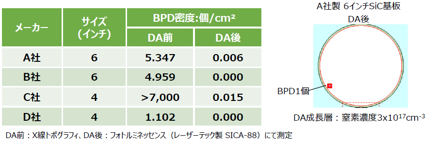
Demonstrated on a commercially available 6-inch SiC wafer:
Dynamic AGE-ing was applied to a commercially available 6-inch SiC wafer.
Currently, 6-inch SiC wafers have a density of thousands of BPDs per cm2.
As a result of applying Dynamic AGE-ing, we confirmed that the number of BPDs that affect device manufacturing can be reduced to one or less within a 6-inch wafer.
The finally formed surface was covered by a BPD-free growth layer.
Even when the epitaxial layer grows, it is only necessary to stack the drift layer.
Productivity can be dramatically improved compared to the conventional method.
What is “AGE”?
Annealing,
Growth,
An acronym for Etching.
–MONOist
https://monoist.atmarkit.co.jp/mn/articles/2103/03/news039.html