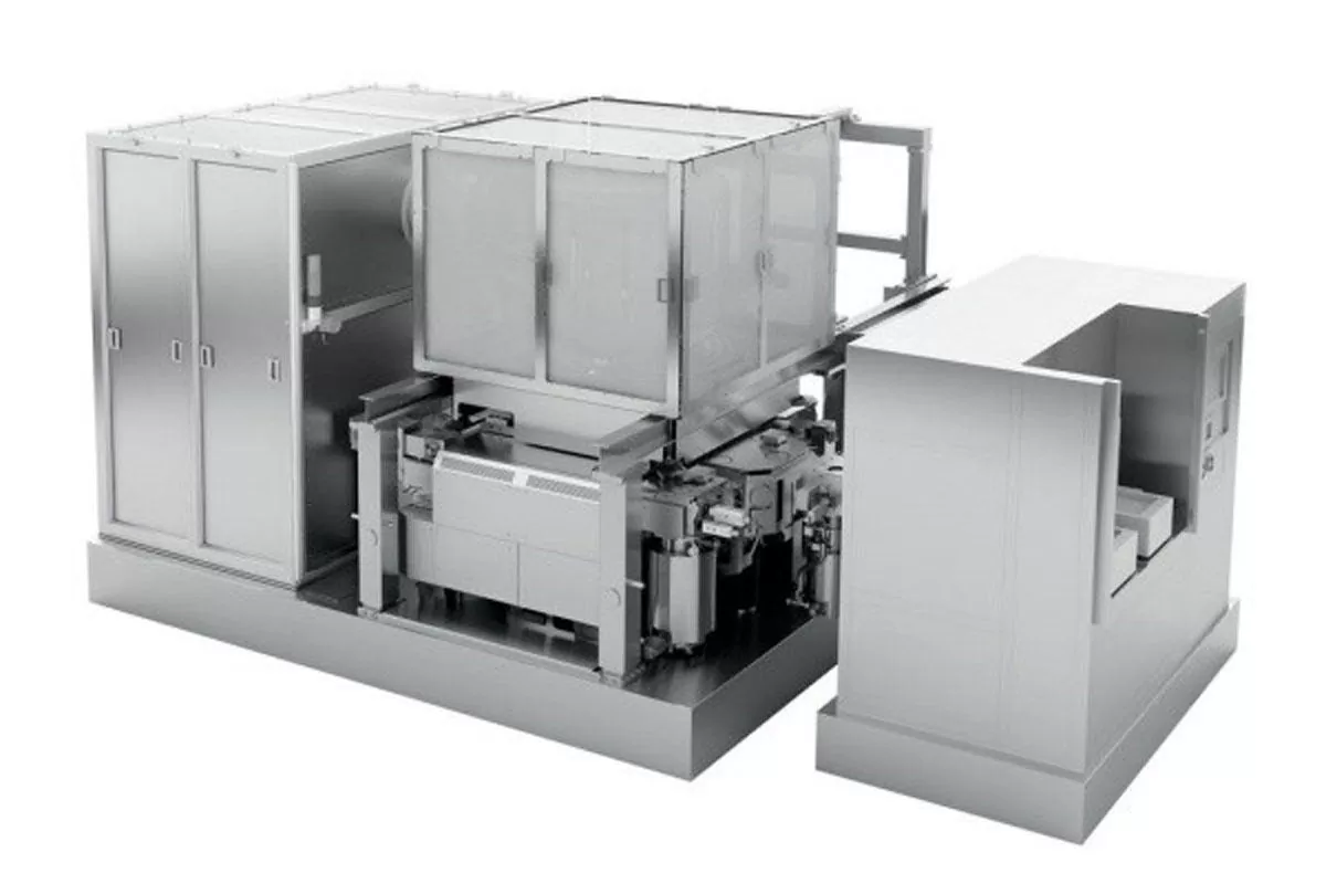
IMS multi-beam mask drawing device (Source: IMS website)
IMS multi-beam mask drawing device (Source: IMS website)
TSMC and Samsung: EUV peripheral technology procurement: drawing equipment, inspection equipment
December 14th
Korea etnews:
EUV lithography peripheral technology:
Electron beam mask drawing device for masks,
Regarding the appearance inspection device for masks,
It is reported that TSMC and Samsung are fighting for battle.
Essential for semiconductor manufacturing:
The production capacity of these devices is lower than that of EUV exposure devices, and it is difficult to procure them.
Even if EUV exposure equipment is available, if these peripherals cannot be secured, it will hinder the manufacture of semiconductor devices using EUV.
EB mask drawing device: IMS Nanofabrication
Austria IMS Nanofabrication is working on a multi-beam EB mask lithography system for EUV.
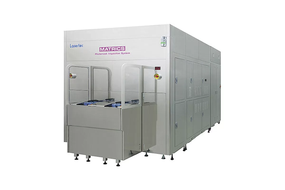
Visual inspection equipment for EUV: Lasertec
On the other hand, the visual inspection equipment for EUV is handled by Lasertec of Japan.
Mynavi News
https://news.mynavi.jp/article/20201217-1597761/
Samsung Electronics and TSMC Looking to Secure Advanced Semiconductor Manufacturing Systems Faster than the Other –
Competition between Samsung Electronics and TSMC to secure equipment necessary for ultra-microfabrication process in addition to EUV (Extreme Ultraviolet) lithography system,
which is only provided by ASML, faster than the other is becoming more intense.
APMI (Actinic Pattern Mask Inspection) system and writer for manufacturing masks are prime examples.
These instruments
are key instruments that will determine productivity and quality when there are increased supplies of chips that are smaller than 5 nanometers.
Both instruments
are also only supplied by a single manufacturer just like EUV lithography system.
According to the industry on Monday, global semiconductor manufacturers such as Samsung Electronics and TSMC
are engaged in a fierce competition in order to secure advanced equipment necessary for ultra-microfabrication process faster than the others.
As EUV lithography process
has recently emerged as the solution for manufacturing next-generation microchips within the global semiconductor industry,
competition to secure ASML’s EUV lithography system
has become a huge topic. ASML is the only company in the world to supply EUV lithography systems that cost more than $137 million (150 billion KRW) per unit.
Electronic beam-based writer
However, there are also other advanced systems
in addition to EUV lithography system that global semiconductor manufacturers are having difficulty to purchase due to lack of suppliers.
Electronic beam-based writer that prints circuit layout onto EUV masks and inspection system that inspects EUV masks whether they can be used are prime examples.
E-beam writer
plays a “brush” role that prints integrated circuit layout onto masks that are absolutely necessary in order to print integrated circuit layouts onto wafers during lithography process.
ArF-based lithography process
E-beam writer manufactured by NuFlare that is based in Japan is currently used for ArF-based lithography process.
However, it is difficult for NuFlare’s E-beam writer to exhibit its full potential under an EUV environment.
Austria-IMS and Japan-Lasertec
The problem is
that both multi-beam writer and APMI system are also made by single company just like EUV lithography system.
Austria-based IMS and Japan-based Lasertec
are the only companies in the world that supply multi-beam writers and EUV mask inspection systems respectively.
ETNews