
DNP: Nanoimprint lithography: Supports 5nm node
-No need for development process of conventional lithography technology-
Dai Nippon Printing (DNP):
Exhibited at “12th High Performance Material Week” (December 8-10, 2021, Makuhari Messe).
Introducing examples of reducing environmental impact, such as carbon neutrality.
-Exhibiting DNP Nanoimprint lithography (NIL)-
Technology of a carbon-free society:
It is an ultra-fine processing technology for semiconductor manufacturing by DNP nanoimprint lithography.
What is NIL:
“Technology that transfers ultra-fine irregularities in nm units by pressing against the substrate material”.
It is based on “Technology of template (plate part) for circuit patterns”.
2003
The company started NIL development in 2003.
2015
In 2015, mass production of NIL started.
2021
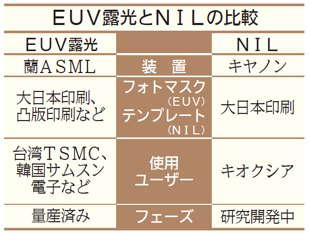
The company, Canon, and Kioxia have cooperated to make it possible to “apply the technology to fine pattern formation in semiconductor manufacturing.”
DNP:
We provide the “template manufacturing technology for circuit patterns” that we have cultivated so far.
Canon:
Responsible for “imprint device technology that transfers in detail” to the circuit pattern board.
Kioxia:
Responsible for “semiconductor manufacturing technology for precision processing” of patterns on substrates.
5nm node process support:
This technology is “compatible with 5nm node generation semiconductor manufacturing processes.”
DNP’s NIL:
The “development process used in conventional lithography technology” becomes unnecessary.
“Significantly low power consumption in the manufacturing process” is possible.
This contributes to carbon neutrality in semiconductor manufacturing.
Nikkei Cross Tech (xTECH)
https://xtech.nikkei.com/atcl/nxt/news/18/11907/
“NIL” developed by Dai Nippon Printing, Kioxia, and Canon
-Semiconductor manufacturing power consumption is 1/10-
Dai Nippon Printing
Kioxia Holdings,
Canon,
Nanoimprint lithography (NIL), which is being jointly developed
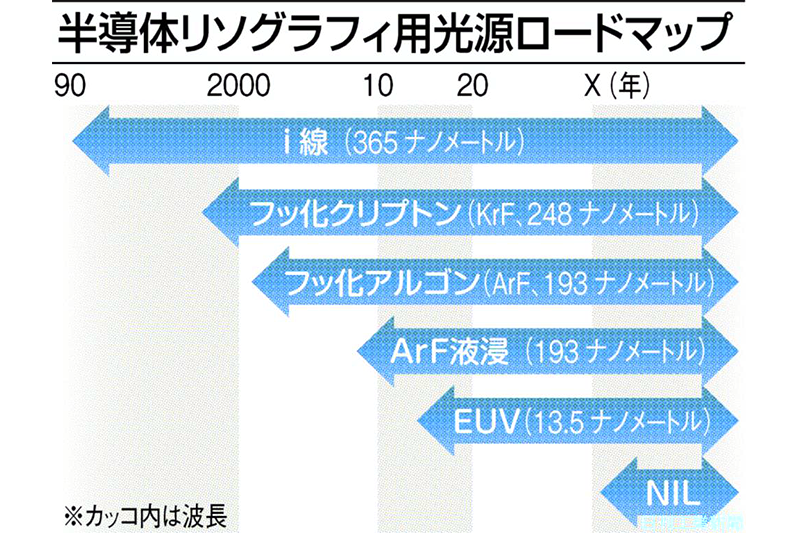
Semiconductor manufacturing at NIL:
It was clarified that “power consumption can be reduced to 1/10 compared to EUV exposure”.
NIL has many problems before mass production, but at present, it has succeeded in forming the most advanced circuit line width.
What is NIL:
NIL presses the mold against the wafer to form a fine circuit pattern.
NIL is for technological development and can handle up to 5 nanometer node circuit line width.
Power consumption is 1/10
Dai Nippon Printing conducted an internal simulation based on the specifications of the equipment in the spring of 2021.
Announced power consumption per wafer in the circuit formation process.
It was found that “it can be reduced to 1/10 compared to the case of using EUV exposure”.
New switch