Semiconductor lithography equipment: More than four times the exposure area!
– For 3D technology: stack multiple chips! ー
Canon:
December 6th,
-For 3D technology that enhances performance by stacking multiple chips-
We have developed a new type of semiconductor lithography system used in post-processing (chipping and packaging).
New semiconductor lithography equipment:
The exposure area is more than four times larger than that of conventional machines.
It corresponds to the production of large advanced semiconductors used for AI.
Focus on 3D technology:
Do not rely on “miniaturization to increase the degree of integration by thinning the circuit”.
He focused on improving 3D technology as a way to improve the performance of semiconductors.
Capture growth by expanding the lineup of compatible models.
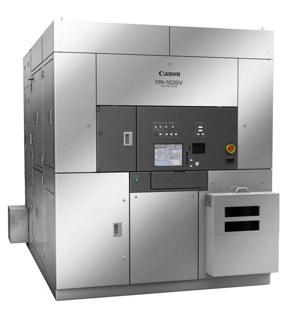
New product FPA-5520iV
LF2 option
New product “FPA-5520iV LF2 option = photo”
Review optical system parts such as lenses,
The homogenizer, which homogenizes the illumination light, has been improved to expand the exposure area.
It becomes easier to respond to the trend toward larger size of advanced semiconductors.
It will go on sale in early January 2023.
Back-end manufacturing process
-Technological areas required in post-process manufacturing processes-
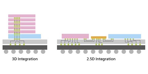
3D technology is:
3D technology is a method of stacking multiple semiconductor chips and connecting them closely.
2.5D technology:
The 2.5D technology “combines multiple chips side by side” and moves them like a single chip.
In recent years, 3D technology has been attracting attention as a method for improving the functionality of semiconductors without relying on miniaturization.
Canon’s “i-line exposure system”:
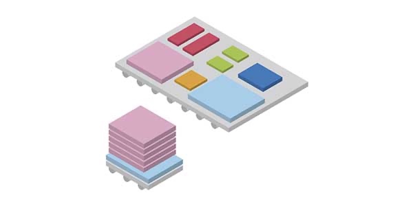
The plate-shaped part on which the chip is mounted by 3D technology has
Wirings for electrically connecting chips are formed in many layers at high density.
Canon’s new exposure tool is used to form this wiring.
Canon’s “i-line exposure device” was applied to the three-dimensional technology and used in the post-process.
new switch
Apparatuur voor halfgeleiderlithografie: meer dan vier keer het belichtingsgebied!
– Voor 3D-technologie: stapel meerdere fiches! ー
Canon:
6 december
-Voor 3D-technologie die de prestaties verbetert door meerdere chips te stapelen-
We hebben een nieuw type halfgeleiderlithografisch systeem ontwikkeld dat wordt gebruikt bij nabewerking (chippen en verpakken).
Nieuwe apparatuur voor halfgeleiderlithografie:
Het belichtingsgebied is meer dan vier keer groter dan dat van conventionele machines.
Het komt overeen met de productie van grote geavanceerde halfgeleiders die worden gebruikt voor AI.
Focus op 3D-technologie:
Vertrouw niet op “miniaturisatie om de mate van integratie te vergroten door het circuit dunner te maken”.
Hij richtte zich op het verbeteren van 3D-technologie als een manier om de prestaties van halfgeleiders te verbeteren.
Profiteer van groei door het assortiment compatibele modellen uit te breiden.
Nieuw product FPA-5520iV
LF2 optie
Nieuw product “FPA-5520iV LF2 optie = foto”
Beoordeel optische systeemonderdelen zoals lenzen,
De homogenisator, die het verlichtingslicht homogeniseert, is verbeterd om het belichtingsgebied uit te breiden.
Het wordt gemakkelijker om in te spelen op de trend naar grotere geavanceerde halfgeleiders.
Het zal begin januari 2023 in de verkoop gaan.
Back-end productieproces
-Technologische gebieden vereist in productieprocessen na het proces-
3D-technologie is:
3D-technologie is een methode om meerdere halfgeleiderchips op elkaar te stapelen en nauw met elkaar te verbinden.
2.5D-technologie:
De 2.5D-technologie “combineert meerdere chips naast elkaar” en verplaatst ze als een enkele chip.
De laatste jaren trekt 3D-technologie de aandacht als een methode om de functionaliteit van halfgeleiders te verbeteren zonder afhankelijk te zijn van miniaturisatie.
Canon’s “i-line belichtingssysteem”:
Het plaatvormige deel waarop de chip is gemonteerd heeft 3D-technologie
Bedradingen voor het elektrisch verbinden van chips worden gevormd in vele lagen met een hoge dichtheid.
Canon’s nieuwe belichtingstool wordt gebruikt om deze bedrading te vormen.
Canon’s “i-line belichtingsapparaat” werd toegepast op de driedimensionale technologie en gebruikt in het nabewerkingsproces.
nieuwe schakelaar
Halbleiter-Lithographie-Anlage: Mehr als viermal so viel Belichtungsfläche!
– Bei 3D-Technologie: Stapeln Sie mehrere Chips! ー
Kanon:
6. Dezember,
-Für 3D-Technologie, die die Leistung durch Stapeln mehrerer Chips verbessert-
Wir haben ein neuartiges Halbleiter-Lithografiesystem entwickelt, das in der Nachbearbeitung (Chipping und Packaging) eingesetzt wird.
Neue Halbleiter-Lithographie-Ausrüstung:
Die Belichtungsfläche ist mehr als viermal größer als bei herkömmlichen Maschinen.
Es entspricht der Produktion großer fortschrittlicher Halbleiter, die für die KI verwendet werden.
Fokus auf 3D-Technologie:
Verlassen Sie sich nicht auf „Miniaturisierung zur Erhöhung des Integrationsgrades durch Verdünnung der Schaltung“.
Er konzentrierte sich auf die Verbesserung der 3D-Technologie, um die Leistung von Halbleitern zu verbessern.
Profitieren Sie vom Wachstum, indem Sie das Angebot an kompatiblen Modellen erweitern.
Neues Produkt FPA-5520iV
LF2-Option
Produktneuheit “FPA-5520iV LF2 Option = Foto”
Überprüfen Sie optische Systemteile wie Linsen,
Der Homogenisator, der das Beleuchtungslicht homogenisiert, wurde verbessert, um den Belichtungsbereich zu erweitern.
Es wird einfacher, auf den Trend zu größeren Abmessungen fortschrittlicher Halbleiter zu reagieren.
Es wird Anfang Januar 2023 in den Handel kommen.
Back-End-Fertigungsprozess
-Technologische Bereiche, die in Post-Process-Fertigungsprozessen benötigt werden-
3D-Technologie ist:
Die 3D-Technologie ist eine Methode, mehrere Halbleiterchips zu stapeln und eng miteinander zu verbinden.
2.5D-Technologie:
Die 2.5D-Technologie “kombiniert mehrere Chips nebeneinander” und bewegt sie wie einen einzigen Chip.
In den letzten Jahren hat die 3D-Technologie als Verfahren zur Verbesserung der Funktionalität von Halbleitern Aufmerksamkeit erregt, ohne auf Miniaturisierung angewiesen zu sein.
Canons „i-line Belichtungssystem“:
Das plattenförmige Teil, auf dem der Chip mittels 3D-Technik montiert ist, hat
Verdrahtungen zum elektrischen Verbinden von Chips werden in vielen Schichten mit hoher Dichte gebildet.
Das neue Belichtungswerkzeug von Canon wird verwendet, um diese Verdrahtung zu bilden.
Canons „i-line Belichtungsgerät“ wurde auf die dreidimensionale Technologie angewendet und in der Nachbearbeitung verwendet.
neuer Schalter
New Canon option for semiconductor lithography system back-end process contributes to 3D advanced packaging technologies, enables mass production of dense circuitry with exposure fields of up to 100 mm x 100 mm
Canon Global
The new FPA-5520iV LF2 Option reduces distortion aberration of less than 1/4 that of its predecessor model, the FPA-5520iV LF Option (released in April 2021),
and features a new projection optical system with greater light level uniformity.
These advancements allow LF2 Option steppers
to provide 0.8 µm resolution across a large 52 mm × 68 mm single-exposure field at while also making possible an ultra-wide 100 mm x 100 mm exposure field.
The FPA-5520iV LF2 Option
inherits the basic performance of the FPA-5520iV, which has the ability to handle warped reconstituted substrates5 an issue which can occur in packaging layers during the mass-production process,
as well as high productivity to enhance availability by detecting alignment marks—even on the reconstituted substrates with large chip array variations.
Going forward,
Canon will strive to support
further technological innovation by expanding its lineup of semiconductor lithography system offerings not only for front-end semiconductor chip manufacturing processes,
but also systems that support state-of-the-art back-end packaging technologies.