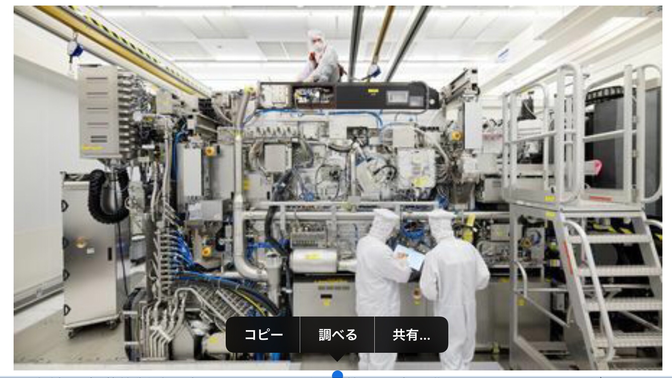
The photo shows the EUV exposure tool at the final stage of assembly (from the ASML website)
Semiconductors in China: Procurement risk of cutting-edge EUV exposure equipment: SMIC delayed by 3 generations
Central Core Integrated Circuit Manufacturing (SMIC):
China’s largest foundry, Zhongshan International Integrated Circuit Manufacturing (SMIC), was listed on the Shanghai Stock Exchange’s new market “Cha-She” in mid-July.
Raised up to 53.2 billion yuan (approx. 808.6 billion yen) and became the largest ever publicly listed market in the science plate market established in July 2019.
SMIC Business Briefing:
On July 6, SMIC held an online business briefing session for institutional investors.
Among them, what attracted the most attention was “Question and answer about SMIC’s EUV (extreme ultraviolet) exposure equipment procurement plan”.
SMIC President:
At this time, it is not necessary to introduce EUV exposure equipment for the production and development of SMIC.
He explained that there is no change in the SMIC procurement plan in the future.
Current SMIC equipment:
The exposure equipment is a core facility for semiconductor manufacturing that prints fine electronic circuits on a silicon wafer.
SMIC has just begun “mass production with 14 nm (nanometer) process technology from the October-December period of 2019.”
We are currently in the process of developing 12nm technology.
Compared to world leading companies, SMIC’s process technology is three generations behind.
New device of TSMC:
The world’s largest Taiwan Integrated Circuit Manufacturing (TSMC) has already started mass production of 5nm in the first half of this year.
Need for new EUV exposure equipment:
SMIC’s current process technology does not require a new EUV exposure tool.
However, new equipment is indispensable for mass production of TSMC 7nm and 5nm in the future.
Dutch ASML:
At the moment, the new EUV exposure system was put into practical use
Only the world’s largest exposure equipment, the ASML in the Netherlands.
Moreover, the number of vehicles produced is less than 30 a year.
For this reason, major semiconductor manufacturers around the world are placing orders.
SMIC support:
In fact, SMIC has also ordered EUV exposure equipment.
Initially, it was scheduled to be delivered at the end of 2019.
However, the introduction has not been realized yet.
The Dutch government’s permission is required to export state-of-the-art exposure equipment.
ASML announced in November 2019 that it is “waiting for permission from the Dutch government”.
SMIC Procurement Risk:
The risk of procurement of state-of-the-art foreign-made equipment and raw materials is the point where investors are most concerned about the future of SMIC.
US Government:
It cannot be denied that increasing export restrictions on Chinese companies may have unpredictable and adverse effects on SMIC’s management in the future.
(Toyo Keizai Online)
https://toyokeizai.net/articles/-/361815?display=b
China semiconductor SMIC listed. Procurement amount, 760 billion yen scale
[Shanghai = Zhang Yuxiang]
Central Core International Integrated Circuit Manufacturing (SMIC)
On the 16th, China’s semiconductor core manufacturing International Core Integrated Circuit Manufacturing (SMIC) has listed its shares on the market “Kaita” for high-tech companies in Shanghai.
SMIC listing background
SMIC, which delisted from the US in 1919, announced its initial public offering at Kaita in May, and went public in two months.
Advanced semiconductor production capacity
In semiconductor manufacturing
- Taiwan Integrated Circuit Manufacturing (TSMC)
- Samsung Electronics of Korea precedes,
- SMIC’s share is only around 5%.
Not only will we be worried about by miniaturization technology, but there will also be a large gap in the production capacity of advanced semiconductors.
Nihon Keizai Shimbun
https://r.nikkei.com/article/DGXMZO61573950W0A710C2FFE000?s=4
TSMC’s N7+ Technology is First EUV Process Delivering Customer Products to Market in High Volume
Hsinchu, Taiwan R.O.C., Oct 7, 2019 –
TSMC (TWSE: 2330, NYSE: TSM)
today announced that its seven-nanometer plus (N7+), the industry’s first commercially available Extreme Ultraviolet (EUV) lithography technology, is delivering customer products to market in high volume.
The N7+ process with EUV technology is built on TSMC’s successful 7nm node and paves the way for 6nm and more advanced technologies.
N7+ is also providing improved overall performance.
When compared to the N7 process, N7+ provides 15% to 20% more density and improved power consumption, making it an increasingly popular choice for the industry’s next-wave products.
TSMC has been quickly deploying capacity to meet N7+ demand that is being driven by multiple customers.
https://www.tsmc.com/tsmcdotcom/PRListingNewsAction.do?action=detail&language=E&newsid=THHIHIPGTH