Semiconductor Equipment in China: Technology Level of Exposure Process
ーExport restrictions on Japanese DUV exposure equipmentー
ー ArFi Immersion Lithography Achieved in China ー
We will deliver the summary from the Yahoo article.
Level of exposure process:
China’s weakest point in semiconductor manufacturing is exposure equipment, which is centered on lithography technology.
What is the exposure process:
Semiconductors have extremely fine wiring drawn on small chips.
Making a wiring pattern by “light irradiation” is called an exposure process.
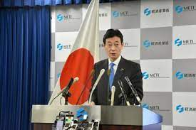
Japan’s export restrictions started:
Japan implemented semiconductor export controls on July 23rd.
It is truly centered on exposure equipment and processes.
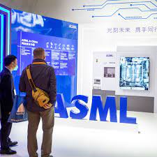
Export of ASML to China:
More than 80% of the world’s major semiconductor manufacturers are ASML customers.
Exports to China account for 15% of the world total.
Traditionally, China and ASML have been on very good terms.
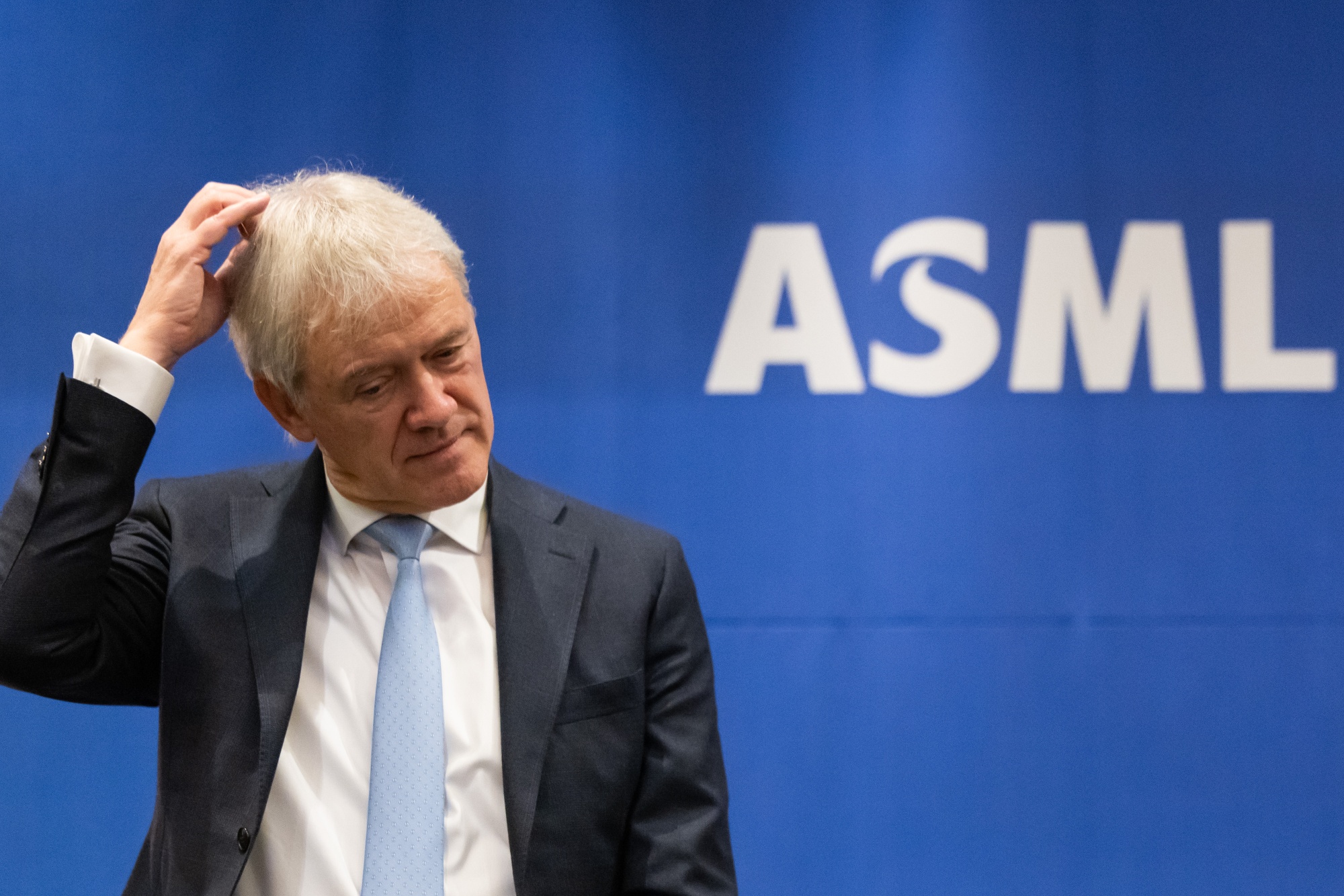
US sanctions against China:
The United States has asked the Netherlands to impose new restrictions on exports of semiconductor equipment to China.
The ASML has been forced into a position of reluctance to align itself with the United States.
It currently accounts for 34.7% of the global market.
ASML’s business locations:
In 2020, we established our own business base in Wuxi High-Tech Park, Jiangsu Province.
ASML has independently developed DUV (deep ultraviolet) exposure equipment for China.
They were planning to launch it in mainland China.
US and Dutch Governments:
In June 2023, the Netherlands decided to ‘enforce the export control law from September 1st’.
The target of this regulation is limited to a small number of high-end DUV and EUV lithography equipment.
ASML leaves “the possibility of releasing a China-only version in China.”
China resents that “ASML is also a victim of the United States.”
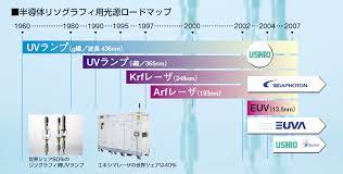
History of the five generations of light sources:
Based on the history of five generations of light sources, China’s development level is analyzed.
g-line: long-wavelength type used in the 1980s
i-line: A slightly shorter wavelength type used in the 1990s
KrF: Krypton-fluorine laser light in the late 1990s
ArF: Laser beam with argon fluoride
EUV: The latest version among the 5 generations
Chinese light source development:
China has successfully developed a light source equivalent to the fourth and a half generation of ArFi.
Chinese Academy of Sciences, Changchun Optical Institute, and Harbin Institute of Technology have successfully developed a 12w DDP-EUV.
The “i” in ArFi stands for “immersion.”
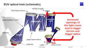
Objective lens development:
The optical system is one of the major components of exposure equipment.
ASML objective lens:
ASML exclusively uses German Zeiss lenses.
Japanese objective lens:
Canon and Nikon have their own lenses. It is advantageous as an optical manufacturer.

Chinese objective lens:
90nm was developed by “Changchun Apu Optical Technology Co., Ltd.”.
“Changchun Optics Office” is developing 32nm EUV lenses.
However, the gap with Zeiss is large.
Dual wafer stage system:
Two wafers can be handled at the same time in one exposure system.
A system that simultaneously performs exposure and measurement.
In Chinese, it is written as “Shuanggutai”.

China’s “shuangtai”:
Tsinghua University and Huazhuo Precision Medicine) achieved 10nm (movement accuracy).
By the way, ASML has been realized down to 2nm.
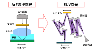
Level of immersion exposure system:
We have developed an immersion exposure system that uses a light source with a short wavelength.
ArF immersion lithography and EUV lithography are what we arrived at.
What is ArF immersion exposure:
An “ArF light source” with a wavelength of 193 nm is used as the light source.
With this technology, patterns can be formed with processing accuracy of the 10-nano generation.
。

Zhejiang Qier Mechatronics:
Zhejiang Qier Mechatronics in China has succeeded in realizing ArFi immersion lithography.
ASML is ahead of China in EUV exposure.
China competes in power semiconductors:
The United States has strengthened sanctions against China in high-end semiconductor manufacturing.
China, on the other hand, will shift to manufacturing middle-class semiconductors with large line widths.
In addition, power semiconductor manufacturing will be strengthened.
Chinese power semiconductors:
In 2020, China’s IGBT (Insulated Gate Bipolar Transistor) self-sufficiency rate was 20%.
By 2024, the self-sufficiency rate is expected to reach 40%.
Effectiveness of US sanctions:
China has already surpassed the United States in space development.
America’s sanctions diplomacy with China has an expiration date.
https://news.yahoo.co.jp/expert/articles/6a65579cd968bf1688062a18f07c0d2e0d6262c1