Canon: Launch of 5nm semiconductor exposure equipment
-Simple structure without optical system-
-5nm node power consumption is 1/10th-
-Create a 3D pattern in one go-
We will deliver a summary of articles published on PC Watch.
Canon’s NIL technology:
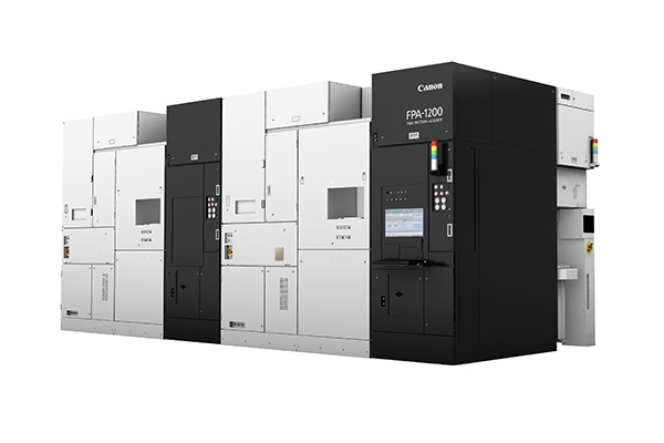
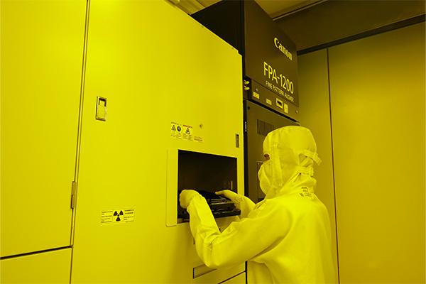
Released the semiconductor manufacturing equipment “FPA-1200NZ2C” that uses unique “nanoimprint” (NIL) technology.
Semiconductor manufacturing equipment: “FPA-1200NZ2C”
The most important element in semiconductor manufacturing is the exposure equipment that transfers circuit patterns onto wafers.
Traditional method:
1. Light is irradiated onto the resist (resin) coated on the wafer.
2. The most common method is to burn the circuit.
However, there is an intervention called the optical system.
Therefore, it relied on “miniaturization based on the wavelength of the light source.”
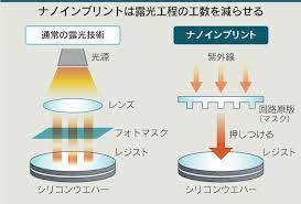
Canon’s NIL technology:
1. A circuit pattern is formed by “pressing a circuit pattern mask” onto the resist on the wafer.
2. By omitting the optical system, it is possible to “faithfully reproduce the fine circuit pattern on the mask.”
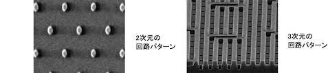
Complex 2D/3D circuit patterns:
2D/3D formation is possible with just one imprint.
Simple structure without optical system:
We developed a simple structure that omitted this optical system.

5nm node power consumption is 1/10:
For cutting-edge logic exposure technology (5nm node/line width 15nm)
Power consumption is 1/10th compared to conventional projection exposure equipment.
It greatly contributes to CO2 reduction.
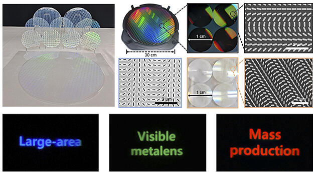
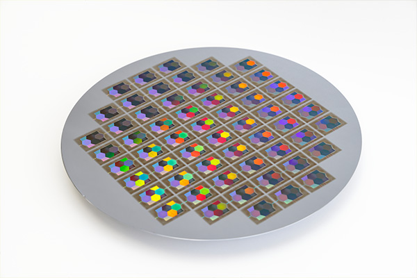
Production of metalens for XR:
Applying “technology that can form 3D patterns in one go” to other fields.
Can be used for “metalens for XR with a fine structure of several tens of nanometers”.
upport for 2nm node:
Currently, it is possible to form patterns with a 5nm node/minimum line width of 14nm, which is at the cutting-edge logic semiconductor manufacturing level.
In the future, by improving the mask, we will be able to support the 2nm node/minimum line width of 10nm.
https://pc.watch.impress.co.jp/docs/news/1538780.html
Nanoimprint lithography semiconductor manufacturing system that covers diverse applications with simple patterning mechanism
Canon Global:
The new product employs newly developed environment control technology
that suppresses the contamination with fine particles in the equipment.

Nanoimprint lithography semiconductor manufacturing system:
This enables high-precision alignment which is necessary for the manufacture of semiconductors
with an increasing number of layers and the reduction of defects due to fine particles,
and enables the formation of fine and complex circuits,
contributing to the manufacture of cutting-edge semiconductor devices.

the manufacture of cutting-edge semiconductor devices:
Since the new product does not require a light source with a special wavelength for fine circuit,
it can reduce power consumption significantly compared to
the photolithography equipment for currently available most advanced logic semiconductors (5-nm-node with 15 nm linewidth),
thereby contributing to CO2 reduction.