Nikon: Supports three-dimensional semiconductors: ArF immersion exposure equipment
-Equipped with “inline Alignment Station (iAS)”-
Nikon:
October 18th
Compatible with advanced semiconductor device manufacturing,
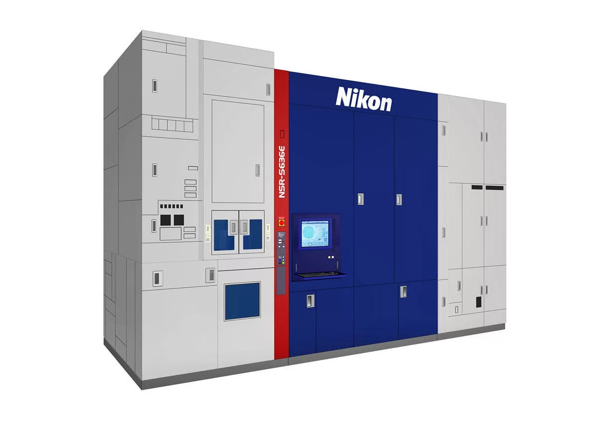
ArF immersion scanner “NSR-S636E”,
Announced that it will be released in 2023.
ArF immersion scanner “NSR-S636E”:
The exposure equipment is equipped with “inline Alignment Station (iAS)”.
With multi-point alignment measurement and higher order correction
Necessary for making the semiconductor device structure three-dimensional,
Aiming for both high polymerization accuracy and high productivity
We have developed an ArF immersion exposure system for 3D.
Areas of use:
Logic semiconductors and memory semiconductors,
CMOS image sensor, etc.
Supports the manufacture of cutting-edge semiconductor devices.
TECH +
https://news.mynavi.jp/article/20211018-2162809/
Nikon Announces Development of the NSR-S636E ArF Immersion Scanner
TOKYO –
Nikon Corporation (Nikon)announced it is currently developing the next-generation NSR-S636E ArF immersion scanner, which will deliver superior overlay accuracy and ultra-high throughput to support manufacturing of the most critical semiconductor devices.
Product sales are scheduled to begin in 2023.
As the digital transformation (DX) accelerates, there is an essential need to process and communicate tremendous volumes of data very quickly.
High-performance semiconductors
are imperative to satisfy these requirements, and semiconductor device technology is progressing with a simultaneous focus on circuit pattern miniaturization as well as 3-dimensional (3D) device structure development
The NSR-S636E features an enhanced inline Alignment Station, or iAS,
which is a wafer pre-measurement module integrated between the coater/developer unit and the lithography scanner.
The S636E and iAS
utilize sophisticated multi-point alignment measurement and high order correction functionsthat enable device makers
to achieve the stringent overlay accuracy necessary for 3D device structures, while also maximizing immersion scanner productivity.The NSR-S636E
is well-suited for cutting-edge semiconductor manufacturing including logic and memory devices, CMOS image sensor applications and more.Nikon | News |
https://www.nikon.com/news/2021/1018_nsr-s636e_01.htm
Alignment Stations – Nikon Precision
https://www.nikonprecision.com/products-and-technology/alignment-stations/