尼康:支持三维半导体:ArF浸入式曝光设备
-配备“在线校准站(iAS)”-
尼康:
10 月 18 日
兼容先进的半导体器件制造,
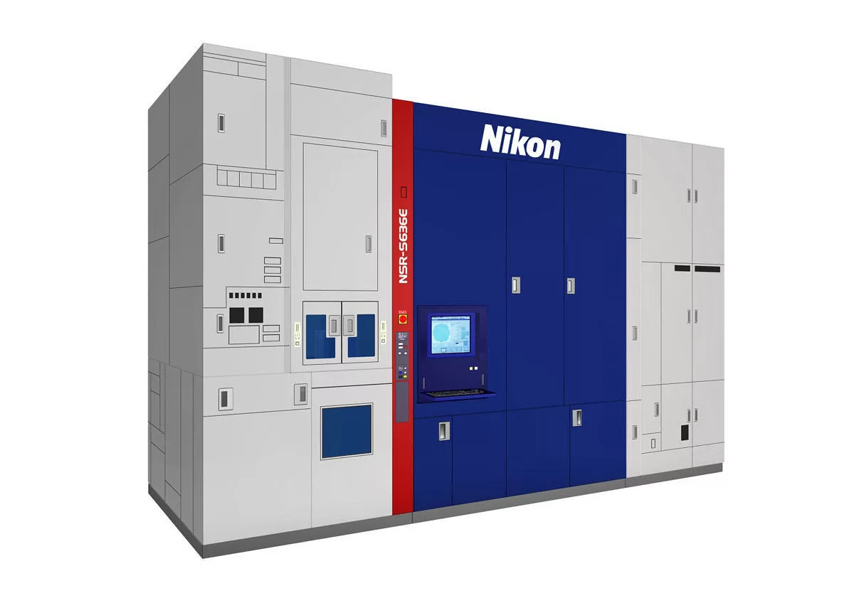
ArF浸入式扫描仪“NSR-S636E”,
宣布将于2023年上映。
ArF 浸入式扫描仪“NSR-S636E”:
曝光设备配备有“在线对准站(iAS)”。
具有多点对准测量和高阶校正
使半导体器件结构立体化所必需的,
以高聚合精度和高生产率为目标
我们开发了用于 3D 的 ArF 浸入式曝光系统。
使用领域:
逻辑半导体和存储半导体,
CMOS图像传感器等
支持尖端半导体器件的制造。
技术+
https://news.mynavi.jp/article/20211018-2162809/
Nikon Announces Development of the NSR-S636E ArF Immersion Scanner
TOKYO –
Nikon Corporation (Nikon)announced it is currently developing the next-generation NSR-S636E ArF immersion scanner, which will deliver superior overlay accuracy and ultra-high throughput to support manufacturing of the most critical semiconductor devices.
Product sales are scheduled to begin in 2023.
As the digital transformation (DX) accelerates, there is an essential need to process and communicate tremendous volumes of data very quickly.
High-performance semiconductors
are imperative to satisfy these requirements, and semiconductor device technology is progressing with a simultaneous focus on circuit pattern miniaturization as well as 3-dimensional (3D) device structure development
The NSR-S636E features an enhanced inline Alignment Station, or iAS,
which is a wafer pre-measurement module integrated between the coater/developer unit and the lithography scanner.
The S636E and iAS
utilize sophisticated multi-point alignment measurement and high order correction functionsthat enable device makers
to achieve the stringent overlay accuracy necessary for 3D device structures, while also maximizing immersion scanner productivity.The NSR-S636E
is well-suited for cutting-edge semiconductor manufacturing including logic and memory devices, CMOS image sensor applications and more.Nikon | News |
https://www.nikon.com/news/2021/1018_nsr-s636e_01.htm
Alignment Stations – Nikon Precision
https://www.nikonprecision.com/products-and-technology/alignment-stations/