DNP Develops Photomask Process Targeting 5nm EUV Lithography
Jul15,2020
Dai Nippon Printing Co., Ltd. (DNP)
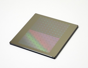
is pleased to announce the development of a photomask process capable of accommodating 5nm Extreme Ultra-Violet (EUV) lithography, a state-of-the-art semiconductor manufacturing process.
The new process employs the multi-beam mask writing tool (MBMW) installed and used by DNP in 2016.
【Overview】
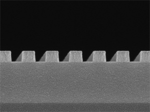
In current semiconductor chip production, circuit patterns are formed on silicon wafers using a photolithography technique.
However, pattern resolution for chip production is limited by the argon fluoride (ArF) wavelength light source. In order to overcome this challenge,
a next-generation lithography technique, EUV lithography with a 13.5nm wavelength light source,
is applied and makes it possible to form circuit patterns with lengths of only several nm.
Commercialization of EUV lithography for microprocessors based on a 5-7nm logic node process, and advanced memory devices,
has begun at a small number of semiconductor chip makers, but is expected to spread to other semiconductor manufacturers engaged in cutting-edge processes.
In 2016,
DNP became the world’s first merchant photomask manufacturer to adopt the MBMW(*1).
In doing so, DNP answered the expectations of semiconductor chip makers with high quality and productivity, including the achievement of a significant shortening in writing time for next-generation photomasks.
In this latest development, by capitalizing on the advantages of MBMW, DNP has successfully developed a photomask process for high-precision EUV lithography capable of accommodating 5nm processes.
What’s New | DNP Group