EUV: Lithography Procurement Competition: TSMC, Samsung, SK Hynix, Intel
-Intel aggressively invests in EUV-
Expanded number of EUV applicable layers:
With the miniaturization of semiconductors, the number of EUV application layers is rapidly increasing.
EUV is currently being introduced in some processes of advanced logic such as the 7 / 5nm generation.
TSMC Trends:
Conventionally, EUV has been applied to four processes in N7.
Currently, EUV application has expanded to 10 processes in N5.
In the future, mass production of N3 is scheduled to start in 2022.
EUV application is expected to expand to 20 processes in the near future.
TSMC overwhelms others in terms of mass production volume.
TSMC’s EUV exposure equipment and the number of units owned are outstanding.
Samsung Electronics:
However, Samsung Electronics plans to “apply EUV exposure equipment in DRAM in addition to advanced logic.”
SK Hynix:
Memory giant SK Hynix has also signed a long-term contract with ASML for purchasing EUV.
Intel Trends:
Intel will also increase EUV-related investment in the future.
March 23 Event:
Clarified that it will continue to manufacture cutting-edge processes at its own fab.
Invest $ 20 billion to build a new plant in Arizona to expand foundry.
In the “7nm generation scheduled for mass production in 2023”
Doubled the number of EUV applicable layers
The idea is to simplify the manufacturing process.
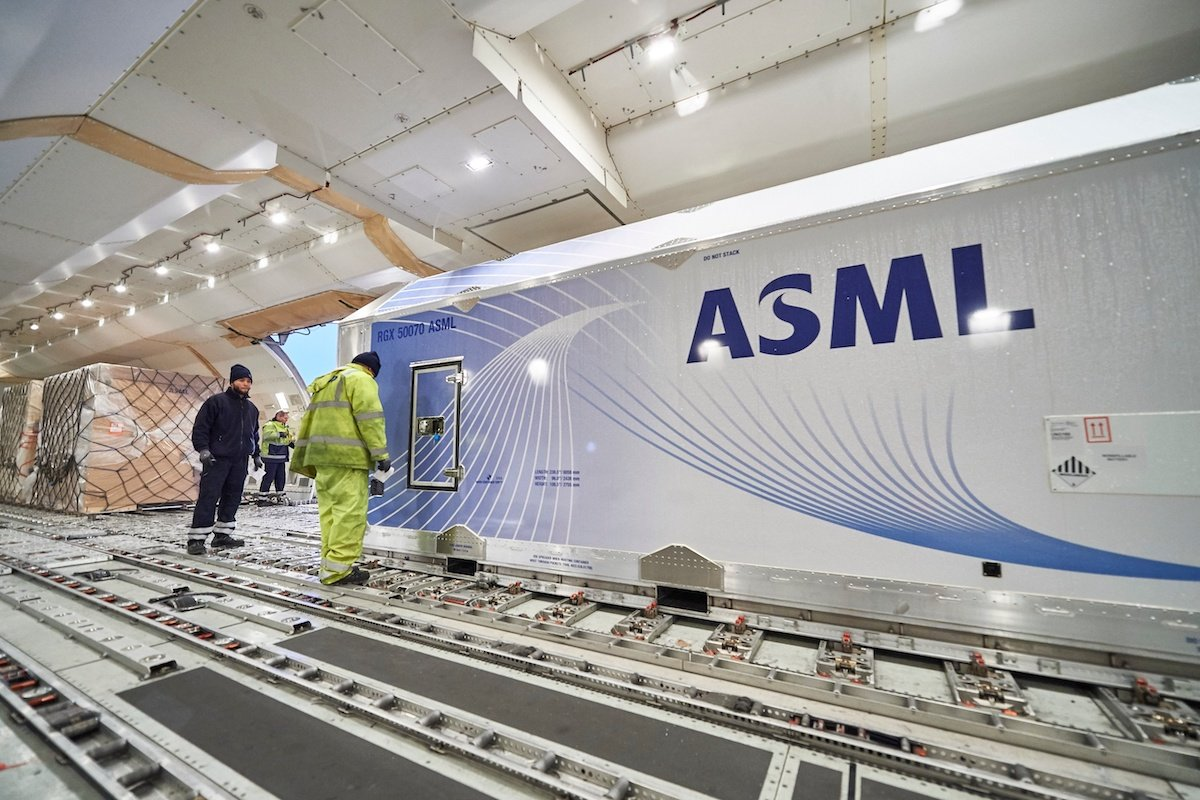
Expected supply of ASML:
ASML plans to “ship over 40 EUV exposure equipment in 2021” for the most important exposure equipment.
As TSMC Samsung accelerates EUV investment, the EUV market demands exceed ASML’s annual manufacturing capacity (40-45 units).
Lasertec supply prospects:
Lasertec has commercialized the world’s only “actic inspection device that can inspect the exposure wavelength with the same EUV light”.
“Lasertec’s supply capacity for mask / blank defect inspection equipment” is also a constraint on the EUV market.
In 2017,
Introduced EUV blanks defect inspection / review equipment to the market.
In 2019
also commercialized “ACTIS A150”, which enables active inspection of patterned masks.
“ACTIS A150”:
“ACTIS A150” is an “essential device for EUV mask inspection with a pellicle (protective film)”.
Lasertec’s supply capacity has received a lot of attention.
ACTIS supply capacity and lead time:
The lead time of ACTIS is very long.
At the February 2021 settlement conference
With suppliers and cooperating factories to shorten delivery time
He revealed that he is proceeding with discussions.
EUV DPT introduction, high NA:
EUV is required to “technological innovation for miniaturization after 3 nm”.
EUV DPT application:
“Application of double patterning (DPT), which is common in optical litho such as ArF,” is being studied.
Higher EUV NA:
Beyond that, “needs for high NA for higher resolution” are also increasing.
Mask / Blanks field:
The transition from the conventional binary mask to the phase shift mask progresses.
imec:
imec has developed a new EUV pellicle product.
For the pellicle that was a concern, we realized “high transmittance based on CNT (carbon nanotube)”.
ASML:
ASML will also announce “Achievements of polysilicon-based, high-transmittance pellicle”.
Significant progress has been made in the mask / blanks field as a whole.
EUV has adopted a technology that is completely different from the conventional optical lithograph.
It is also positioned as a major business opportunity in the equipment and materials fields.
LIMO