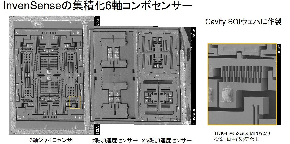
InvenSense 6-axis combo sensor. A combo of XYZ axis accelerometer and 3 axis gyro. Made with “Cavity SOI” with a special cavity
Intel: Whereabouts of semiconductor / MEMS market: Disparity with TSMC
-Commentary by Professor Tanaka of Tohoku University-
Professor Tanaka, Tohoku University:
Professor Tanaka of Tohoku University explained the whereabouts of the semiconductor / MEMS market.
At the event, Professor Tanaka said, “The difference in manufacturing technology between Intel and TSMC is widening.”
Intel, the “champion” of the semiconductor industry, and TSMC, the largest semiconductor contract factory.
What are the current locations of both parties?
From the latest trends in semiconductors and MEMS,
Even proposals for the revival of the domestic manufacturing industry
Summarize the content of Mr. Tanaka’s lecture.
A. “Champion” Intel’s impatience
-The difference in technical capabilities with TSMC is clear-
Intel’s Anguish:
Intel has long reigned as the king of semiconductor manufacturers.
Intel is positioned as an IDM (Integrated Device Manufacturer) and consistently carries out all semiconductor processes in-house.
But Intel has been in a difficult situation in recent years.
Since 2016, it has taken time to supply CPU due to the yield problem of 10nm process.
Furthermore, it caused a “memory recession” in which the price of memory plummeted.
In 2020, it was reported that NVIDIA’s market capitalization exceeded Intel.
Rise of NVIDIA:
NVIDIA is known as “a fabless manufacturer of general-purpose GPUs that are attracting attention in AI.”
fabless is a manufacturing industry that does not own a production plant.
Qualcomm, Broadcom, Apple and others are actually fabless semiconductor manufacturers.
Intel, still 7nm process:
Intel has been a leader in the “miniaturization” of semiconductor manufacturing.
However, They are currently struggling to launch the 7nm process.
TSMC Leads in 3nm Process:
TSMC plans to start production of 3nm process CPUs in 2022.
The gap in manufacturing technology is widening.
In general, the finer the process, the lower the power consumption.
The difference in manufacturing technology is not limited to miniaturization technology.
TSMC Chiplet Technology:
CPUs for servers are not composed of microchips, but are manufactured by dividing them into multiple functional parts.
Manufactured side by side on an interposer (a substrate that conducts front and back circuits with through electrodes).
This method, called chiplet technology, is drawing attention as a new approach.
Intel is also behind TSMC in this chiplet technology.
If the gap continues to widen, Intel may give up on research and development of cutting-edge semiconductor processes.
B. Frustration of the US government
-Attracting TSMC factories and focusing on semiconductor manufacturing-
The US government feels a strong sense of crisis in this situation.
“Once the research and development of cutting-edge semiconductor processes is stopped, it cannot be resumed later,” he said.
In the future, there is a risk that the United States will become a country that can design semiconductors but cannot manufacture semiconductors themselves.
Attract TSMC to the US:
The impatient US government will invite a factory in TSMC, Taiwan, to Arizona.
Production is scheduled to begin in 2024 on the latest line of the 5nm process.
However, it is expected that “TSMC’s 3nm process will be the mainstream by the time the production line starts in 2024.”
The US factory “is no longer at the cutting edge at that point.”
Taiwanese Government’s Plan:
The Taiwanese government will present a small TSMC factory to the United States.
“That’s why They can get security and diplomatic incentives from the US government.”
Pit of fabless model:
The United States “has fallen into a big pitfall due to the great success of the fabless model.”
“Take abandoned by disregarding semiconductor manufacturing” has come to the United States.
It is in-kind capital intensive,
It’s muddy,
It doesn’t turn around,
They downplayed the importance of semiconductor manufacturing technology.
Decline in US Semiconductor Manufacturing Technology:
But in the United States
It is undeniable that “easy work on a computer has been touted rather than physical manufacturing.”
The design field has long been emphasized in the research of well-known American universities.
“Intel was not able to launch the 5nm process satisfactorily” is largely a reflection of “the immaturity of semiconductor manufacturing technology in the United States.”
“The best students in the United States have shunned the semiconductor manufacturing field.”
Taiwan semiconductor manufacturing level is outstanding:
On the other hand, in Taiwan
It is a well-known fact that “the best Taiwanese youth get a job at TSMC”.
Also,
“The microfabrication facility of the Taiwan semiconductor manufacturing plant is one of the most advanced workplaces in DX.”
In other words, it can be said that this semiconductor manufacturing technology is now saving Taiwan.
C. MEMS fabless model
-“Manufacturing process” is an important key-
“MEMS” (Micro Electro Mechanical Systems), which is also one of the fabless model forms
Machine element parts and
sensor,
Actuator,
Electronic circuits, etc.
“MEMS” is integrated on one silicon substrate or lath substrate.
Again, the on-site manufacturing process plays an important role.
Semiconductor design and manufacturing technology:
These are the two wheels of the car, and the distance that one wheel can run is not long.
Needless to say, it is important to constantly improve microfabrication technology in line with on-site manufacturing.
Successful fabless MEMS:
The most famous success story for fabless MEMS is InvenSense in the United States.
Founded in 2003, InvenSense is growing at an alarming rate.
After IPO in NY market in 2011
TDK acquired it for 150 billion yen in 2016.
InvenSense MEMS Sensors:
This MEMS wafer is said to differ from the conventional method in the following points.
Join the ASIC wafers and
While electrically joining MEMS and ASIC
At the same time, packaging MEMS at the wear level
InvenSense product excellence:
You can also “make a 3-axis accelerometer and a gyro sensor at the same time”.
In other words, the 6-axis combo sensor becomes very small.
InvenSense products have been accepted in game consoles and smartphones.
Business + IT