Semiconductor: Development of EUV peripherals: Lasertec, Tokyo Electron
EUV exposure of semiconductors:
The presence of Japanese equipment manufacturers is increasing in the peripheral process of “extreme ultraviolet (EUV) exposure”, which is indispensable for miniaturization of semiconductor circuits.
Presence of ASML:
ASML monopolizes the most important exposure equipment.
On the other hand, Japanese manufacturers have a high share in the field of peripheral equipment such as inspection and application / development of photosensitizers.
However, advanced EUV-related equipment is expensive, and the investment burden is heavy for semiconductor manufacturers.
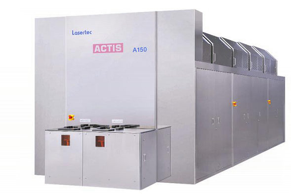
Lasertec in Japan:
Lasertec, which handles EUV inspection equipment.
Orders for semiconductor-related equipment in the July-September period increased 2.6 times year-on-year.
In response to increasing demand, we are currently increasing the number of business partners that outsource production.
The company holds a 100% share of the defect inspection equipment for EUV exposure photomasks (original plates of semiconductor circuits).
Current EUV exposure mask inspection:
Currently, deep ultraviolet (DUV) light is used as a light source in EUV exposure mask inspection.
However, EUV light has a shorter wavelength than DUV light and has higher defect detection sensitivity.
Support for 5 nanometers:
At present, the state-of-the-art circuit line width of 5 nanometers can be used with DUV light.
Support for 2 nanometers:
However, miniaturization will progress in the future, and it will reach the level of 2 nanometers.
According to Lasertec Misawa Corporate Planning Office Manager
“DUV light does not have enough sensitivity,” he said.
“Demand for inspection equipment that uses EUV light as a light source” will increase.
Tokyo Electron:
100% share in coater / developer (coating and developing equipment) for EUV.
Tokyo Electron: President Toshiki Kawai
In the future, with the introduction of new EUV, “technological innovation in the entire process” will progress.
The number of processes in “fields not directly related to EUV” will also increase.
Expected to have a ripple effect on peripheral processes such as “film forming equipment and etching equipment”.
Foundry (contract manufacturing of semiconductors):
Taiwan TSMC:
Utilizing EUV,
In the spring of 2020, mass production of semiconductors with a circuit line width of 5 nanometers began.
Mass production of 3 nanometer semiconductors is scheduled to start in 2022.
Samsung Electronics Korea:
Mass-produce 5 nanometer semiconductors.
In the future, EUV is expected to be applied to DRAM in addition to the conventional logic ICs, and its introduction can be expected to expand.
Hitachi High-Tech: Managing Director Ishiwa
“The limit of economic rationality comes before the limit of miniaturization technology.”
Semiconductor performance improvement:
“Technology for vertically stacking multiple semiconductor chips, such as three-dimensionalization,” will appear.
There is also a growing movement to improve the performance of semiconductors by methods other than miniaturization.
New switch