Tokyo Electron: Provided to ASML: Next Generation Coater / Developer
Tokyo Electron:
On June 8, it announced plans to supply next-generation equipment to the imec-ASML High NA EUV Laboratory.
ASML’s EUV exposure equipment-combined with next-generation machines.
Tokyo Electron
From the research and development stage, we will work with the world’s top miniaturization technology companies to enhance development competitiveness.
imec-ASML Joint EUV Institute:
Tokyo Electron will supply the equipment to the imec-ASML High NA EUV Laboratory (Veldhoven City)
We are proud of the world’s top level in R & D of semiconductor circuit line width miniaturization technology.
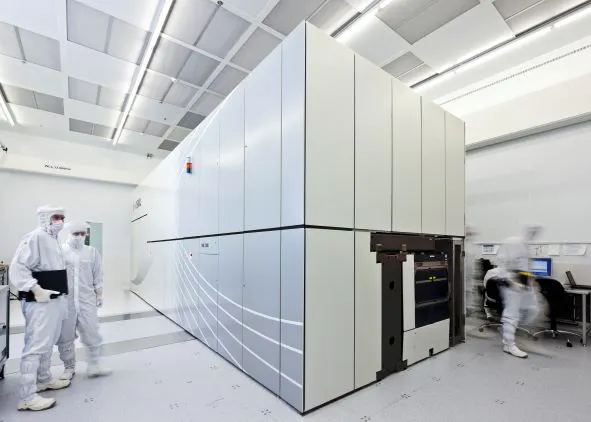
Coater / Developer provided:
Tokyo Electron provides Coater / Developer (coating and developing equipment) that coats and develops photoresists on semiconductors.
This is the first time that the equipment has been shipped to the imec-ASML laboratory.
Tokyo Electron will increase its competitive advantage by digging into the research and development of cutting-edge semiconductors.
Tokyo Electron’s global market share:
According to research firm Global Net
Tokyo Electron is a Coater / Developer with a 90% global market share.
Tokyo Electron has a 100% share for EUV exposure equipment.
Purpose of joint research:
ASML’s next-generation EUV exposure system and
Tokyo Electron’s coating and developing equipment,
Integrate and integrate
Aim to improve semiconductor productivity.
Full-scale operation time:
Tokyo Electron’s equipment will be supplied in the first half of 2022.
The combined equipment is planned to be put into operation in 2023.
When to adopt TSMC:
TSMC is currently developing “3 nano products.”
TSMC plans to start mass production of “3 nano products” in the latter half of 2022.
The next-generation EUV exposure equipment developed this time will be applied to mass production of this “3 nano product” and beyond.
Collaborative company with imec:
imec is focusing on research toward semiconductor miniaturization.
JSR
A joint venture with imec, which produces photoresists for EUV.
Dai Nippon Printing (DNP)
In collaboration with imec, we are developing photomasks for next-generation semiconductors.
Development of miniaturization technology
Collaboration with ASML and imec, which have EUV-related technologies, is the key to maintaining a competitive advantage.
Nihon Keizai Shimbun
https://www.nikkei.com/article/DGXZQOUC08CP10Y1A600C2000000/
Tokyo Electron to Collaborate with imec-ASML Joint High NA EUV Research Laboratory
Tokyo Electron announced today
the company will introduce its leading-edge Coater/Developer to the imec-ASML joint high NA EUV research laboratory in Veldhoven, the Netherlands.
The equipment
will be integrated inline* with EXE:5000, ASML’s next-generation high NA EUV lithography system with a 0.55 numerical aperture (NA), scheduled to be operational in 2023.
By collaborating with imec and ASML,
TEL will continue to pursue technological development to meet the ongoing scaling needs of its customers.
High NA EUV lithography
is expected to provide more advanced pattern scaling solutions compared to conventional EUV lithography.
The Coater/Developer being introduced to the joint high NA lab
will feature advanced capabilities which are not only compatible with widely used chemically amplified resists and underlayers,
but are also compatible with spin-on metal-containing resists.
Spin-on metal-containing resists
have demonstrated high resolution and high etch resistance, and are expected to enable finer patterning.
However, metal-containing resists
also require sophisticated pattern size control as well as metal contamination control on the backside and bevel of the wafer.
To meet these challenges,
the Coater/Developer being installed at the joint high NA lab comes with leading-edge process modules capable of handling metal-containing resists.
Combined with the new process modules, a single unit of TEL Coater/Developer
can process a wide variety of materials inline, including chemically amplified resists, metal-containing resists, and underlayers.
This will enable flexible fab operation, while also realizing increased productivity and high availability that are among the advantages of a Coater/Developer.
Yoshinobu Mitano, TEL Corporate Director, Senior Vice President and General Manager of SPE Business Division,
said,
“TEL is honored to collaborate with imec and ASML at the joint high NA lab to further understand and solve the challenges of high EUV NA patterning. By leveraging our experience in high volume manufacturing of EUV lithography process technology, we intend to deliver high NA EUV process solutions to our customers’ fabs in a timely manner.”
Notification | Tokyo Electron Ltd.
https://www.tel.com/news/topics/2021/20210608_001.html?_fsi=TmlRzK43