Tokyo Electron: 提供给 ASML: Next Generation Coater / Developer
东京电子:
6 月 8 日,它宣布计划向 imec-ASML 高 NA EUV 实验室供应下一代设备。
ASML 的 EUV 曝光设备 – 与下一代机器相结合。
东京电子
从研发阶段,我们将与世界顶级微型化技术公司合作,提升开发竞争力。
imec-ASML 联合 EUV 研究所:
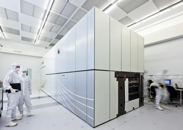
东京电子将为imec-ASML High NA EUV实验室(维尔德霍芬市)提供设备
我们以在半导体电路线宽小型化技术研发方面处于世界顶级水平而自豪。
提供涂布机/显影剂:
东京电子提供在半导体上涂布和显影光刻胶的 Coater/Developer(涂布和显影设备)。
这是该设备首次运往imec-ASML实验室。
东京电子将通过深入研究和开发尖端半导体来增加其竞争优势。
东京电子的全球市场份额:
根据研究公司 Global Net
Tokyo Electron 是一家拥有 90% 全球市场份额的涂布机/开发商。
东京电子拥有 EUV 曝光设备 100% 的份额。
联合研究目的:
ASML 的下一代 EUV 曝光系统和
东京电子的涂装和显影设备,
整合与整合
旨在提高半导体生产率。
满量程运行时间:
东京电子的设备将于2022年上半年供货。
组合设备计划于2023年投产。
何时采用台积电:
台积电目前正在开发“3纳米产品”。
台积电计划在2022年下半年开始量产“3纳米产品”。
此次开发的下一代EUV曝光设备将应用于这款“3纳米产品”及以后的量产。
与imec合作的公司:
imec 专注于半导体小型化的研究。
JSR
与imec的合资企业,生产EUV光刻胶。
大日本印刷 (DNP)
我们正在与 imec 合作开发用于下一代半导体的光掩模。
小型化技术的发展
与拥有 EUV 相关技术的 ASML 和 imec 的合作是保持竞争优势的关键。
日本经济新闻
https://www.nikkei.com/article/DGXZQOUC08CP10Y1A600C2000000/
Tokyo Electron to Collaborate with imec-ASML Joint High NA EUV Research Laboratory
Tokyo Electron announced today
the company will introduce its leading-edge Coater/Developer to the imec-ASML joint high NA EUV research laboratory in Veldhoven, the Netherlands.
The equipment
will be integrated inline* with EXE:5000, ASML’s next-generation high NA EUV lithography system with a 0.55 numerical aperture (NA), scheduled to be operational in 2023.
By collaborating with imec and ASML,
TEL will continue to pursue technological development to meet the ongoing scaling needs of its customers.
High NA EUV lithography
is expected to provide more advanced pattern scaling solutions compared to conventional EUV lithography.
The Coater/Developer being introduced to the joint high NA lab
will feature advanced capabilities which are not only compatible with widely used chemically amplified resists and underlayers,
but are also compatible with spin-on metal-containing resists.
Spin-on metal-containing resists
have demonstrated high resolution and high etch resistance, and are expected to enable finer patterning.
However, metal-containing resists
also require sophisticated pattern size control as well as metal contamination control on the backside and bevel of the wafer.
To meet these challenges,
the Coater/Developer being installed at the joint high NA lab comes with leading-edge process modules capable of handling metal-containing resists.
Combined with the new process modules, a single unit of TEL Coater/Developer
can process a wide variety of materials inline, including chemically amplified resists, metal-containing resists, and underlayers.
This will enable flexible fab operation, while also realizing increased productivity and high availability that are among the advantages of a Coater/Developer.
Yoshinobu Mitano, TEL Corporate Director, Senior Vice President and General Manager of SPE Business Division,
said,
“TEL is honored to collaborate with imec and ASML at the joint high NA lab to further understand and solve the challenges of high EUV NA patterning. By leveraging our experience in high volume manufacturing of EUV lithography process technology, we intend to deliver high NA EUV process solutions to our customers’ fabs in a timely manner.”
Notification | Tokyo Electron Ltd.
https://www.tel.com/news/topics/2021/20210608_001.html?_fsi=TmlRzK43