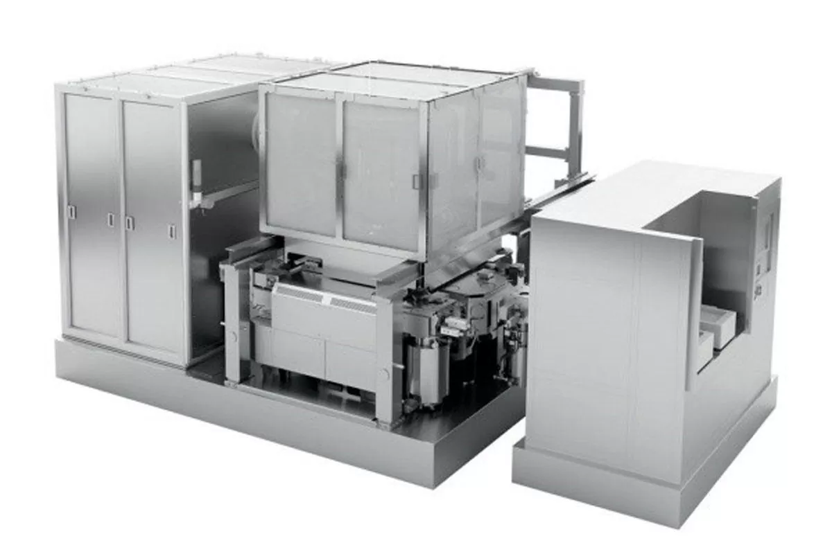
IMSのマルチビーム方式のマスク描画装置 (出所:IMS Webサイト)
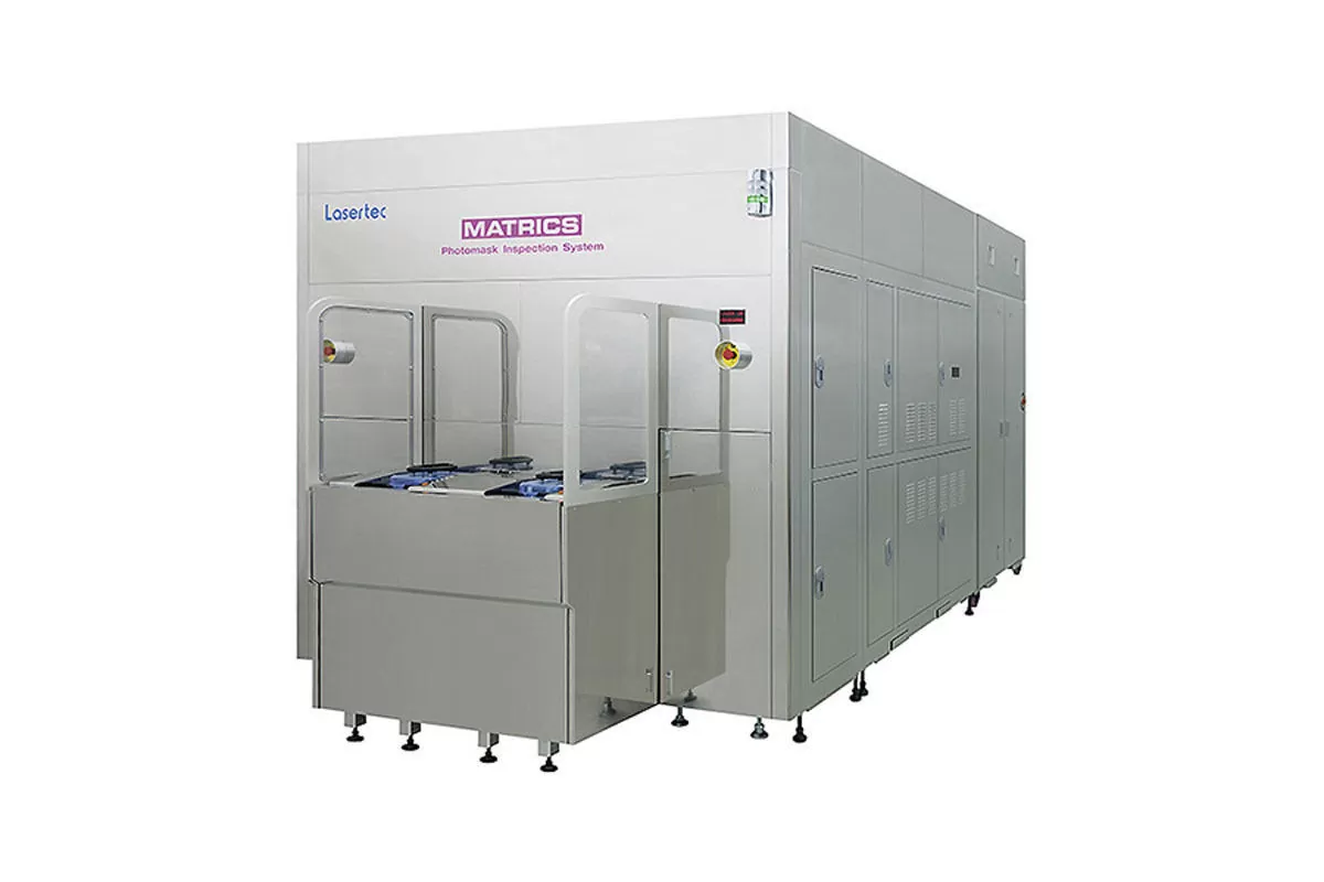
レーザーテックのマスク検査装置 (出所:レーザーテックWebサイト)
TSMCとSamsung:EUVの周辺技術調達:描画装置、検査装置(動画):
TSMC・Samsung: EUV peripheral procurement: drawing,inspection:
台积电和三星:EUV的外围技术采购:制图设备,检查设备
12月14日
韓国etnews:
EUVリソグラフィの周辺技術:
- マスク向け電子ビームマスク描画装置と、
- マスクの外観検査装置についても、
TSMCとSamsungが争奪戦を繰り広げていると報じている。
半導体製造に不可欠:
これらの装置の生産能力は、EUV露光装置よりも低く、調達しずらい。
仮に、「EUV露光装置を入手できたとしても、これらの周辺装置を確保できなければ、EUVを用いた半導体デバイスの製造に支障をきたす」とのこと。
EBマスク描画装置:IMS Nanofabrication
EUV向けマルチビーム方式のEBマスク描画装置はオーストリアIMS Nanofabricationが手掛けている。
EUV向け外観検査装置:レーザーテック
一方のEUV向け外観検査装置は、日本のレーザーテックが手掛けている。
マイナビニュース
https://news.mynavi.jp/article/20201217-1597761/
Samsung Electronics and TSMC Looking to Secure Advanced Semiconductor Manufacturing Systems Faster than the Other –
Competition between Samsung Electronics and TSMC to secure equipment necessary for ultra-microfabrication process in addition to EUV (Extreme Ultraviolet) lithography system,
which is only provided by ASML, faster than the other is becoming more intense.
APMI (Actinic Pattern Mask Inspection) system and writer for manufacturing masks are prime examples.
These instruments
are key instruments that will determine productivity and quality when there are increased supplies of chips that are smaller than 5 nanometers.
Both instruments
are also only supplied by a single manufacturer just like EUV lithography system.
According to the industry on Monday, global semiconductor manufacturers such as Samsung Electronics and TSMC
are engaged in a fierce competition in order to secure advanced equipment necessary for ultra-microfabrication process faster than the others.
As EUV lithography process
has recently emerged as the solution for manufacturing next-generation microchips within the global semiconductor industry,
competition to secure ASML’s EUV lithography system
has become a huge topic. ASML is the only company in the world to supply EUV lithography systems that cost more than $137 million (150 billion KRW) per unit.
Electronic beam-based writer
However, there are also other advanced systems
in addition to EUV lithography system that global semiconductor manufacturers are having difficulty to purchase due to lack of suppliers.
Electronic beam-based writer that prints circuit layout onto EUV masks and inspection system that inspects EUV masks whether they can be used are prime examples.
E-beam writer
plays a “brush” role that prints integrated circuit layout onto masks that are absolutely necessary in order to print integrated circuit layouts onto wafers during lithography process.
ArF-based lithography process
E-beam writer manufactured by NuFlare that is based in Japan is currently used for ArF-based lithography process.
However, it is difficult for NuFlare’s E-beam writer to exhibit its full potential under an EUV environment.
Austria-IMS and Japan-Lasertec
The problem is
that both multi-beam writer and APMI system are also made by single company just like EUV lithography system.
Austria-based IMS and Japan-based Lasertec
are the only companies in the world that supply multi-beam writers and EUV mask inspection systems respectively.
ETNews