DNP:5nm対応 フォトマスクプロセス開発:EUVリソグラフィ向け(動画):
DNP Develops Photomask Process Targeting 5nm EUV Lithography:
DNP:开发了5nm兼容的光掩模工艺:用于EUV光刻
2020年7月10日
大日本印刷(DNP):
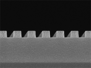
マルチ電子ビームを使うマスク描画装置を利用し、現在の半導体製造の最先端プロセスであるEUV(Extreme Ultra-Violet:極端紫外線)リソグラフィに対応します、
5ナノメートル(nm:10-9m)プロセス相当のフォトマスク製造プロセスを開発しました。
【5nmの最先端半導体用フォトマスク製造技術の特長】
フォトリソグラフィ:欠点
現在の半導体製造では、フォトリソグラフィ技術で、十数nmの回路パターンをシリコンウェハに形成しています。
しかし、フォトリソグラフィ技術では、光源に、波長が193nmのArF(フッ化アルゴン)等のエキシマレーザーを使用しているため、解像度に限界がありました。
EUVリソグラフィ:長所
この課題に対し、EUVリソグラフィでは、波長が13.5nmのEUVを光源とすることで、数nmの回路パターンの形成が可能になります。
このEUVリソグラフィ技術は、一部の半導体メーカーで、5~7nmプロセスのマイクロプロセッサーや最先端メモリデバイス等での実用化が始まっています。
今後の計画:
DNPは
- 国内外の半導体メーカーのほか、
- 半導体開発コンソーシアム、
- 製造装置メーカー、
- 材料メーカー等へ
EUVリソグラフィ向けフォトマスクを提供。
2023年には年間60億円の売上げを目指します。
IMEC(Interuniversity Microelectronics Centre)
ベルギーに本部を置く半導体の国際研究機関IMEC(Interuniversity Microelectronics Centre)をはじめとした
パートナーとの共同開発を通じて、3nm以降のより微細なプロセス開発を進めていきます。
ニュース | DNP 大日本印刷
https://www.dnp.co.jp/news/detail/10158409_1587.html
DNP Develops Photomask Process Targeting 5nm EUV Lithography
Jul15,2020
Dai Nippon Printing Co., Ltd. (DNP)
is pleased to announce the development of a photomask process capable of accommodating 5nm Extreme Ultra-Violet (EUV) lithography, a state-of-the-art semiconductor manufacturing process.
The new process employs the multi-beam mask writing tool (MBMW) installed and used by DNP in 2016.
【Overview】
In current semiconductor chip production, circuit patterns are formed on silicon wafers using a photolithography technique.
However, pattern resolution for chip production is limited by the argon fluoride (ArF) wavelength light source. In order to overcome this challenge,
a next-generation lithography technique, EUV lithography with a 13.5nm wavelength light source,
is applied and makes it possible to form circuit patterns with lengths of only several nm.
Commercialization of EUV lithography for microprocessors based on a 5-7nm logic node process, and advanced memory devices,
has begun at a small number of semiconductor chip makers, but is expected to spread to other semiconductor manufacturers engaged in cutting-edge processes.
In 2016,
DNP became the world’s first merchant photomask manufacturer to adopt the MBMW(*1).
In doing so, DNP answered the expectations of semiconductor chip makers with high quality and productivity, including the achievement of a significant shortening in writing time for next-generation photomasks.
In this latest development, by capitalizing on the advantages of MBMW, DNP has successfully developed a photomask process for high-precision EUV lithography capable of accommodating 5nm processes.
What’s New | DNP Group