東芝:トリプルゲートIGBTを開発:損失を4割削減(動画):
Toshiba: Developed triple gate IGBT: Reduced loss by 40%:
东芝:开发三栅极IGBT:损耗降低40%
ー3つのゲート電極でスイッチング損失を4割削減ー
2021-06-02
東芝:
2021年6月2日、「トリプルゲートIGBT」を開発しました。
IGBT(Insulated Gate Bipolar Transistor)とは、インバーターやDC-DCコンバーターなどの電力変換器用パワー半導体です。
電力のオンとオフ切替時の損失を、従来比で最大40.5%低減できます。
2023~2024年製品化:
今後、信頼性の確認など実用化に向けた開発を進めて、2023~2024年に製品化する予定。
「ISPSD2021」で発表:
今回の研究成果は、パワー半導体の国際学会「ISPSD2021」(2021年5月30日~6月2日、オンライン開催)で発表される。
東芝 研究開発センター
電子デバイス室長・高尾和人氏今回のトリプルゲートIGBTは、「従来の性能飽和の壁をブレークスルーするものになり得る」と語りました。
今日のニュース
https://jp.rwwiki.cn/finances/57745.html
Toshiba’s Triple-Gate IGBT Power Semiconductors Cut Switching Power Losses by 40.5%
-Support high efficiency power converters for electrical systems and contribute to the realization of carbon-neutral economy-
2 June, 2021
Toshiba Corporation TOKYO─
Toshiba Corporation (TOKYO: 6502) has developed a prototype triple-gate IGBT*1
that reduces overall power loss by up to 40.5% when switching on and off (switching losses), the process of allowing and stopping electricity flow, in power semiconductors used to control electric power.
It is difficult to reduce power loss in IGBT,
due to a trade-off whereby reducing the loss when the IGBT is on (conduction losses) increases switching loss.
Toshiba took on this problem
by developing a silicon IGBT with a new structure of three gate electrodes and gate control technology that delivers high accuracy gate electrode switching.
The new device
reduces turn-on loss*2 by 50% and turn-off loss*3 by 28%,
an overall reduction of up to 40.5% against a conventional single-gate electrode IGBT, with no increase in conduction losses.
The new technology is expected to boost the efficiency of power converters in electrical systems,
including renewable energy systems, electric vehicles, railroads, and industrial equipment.
Toshiba will present the technology at ISPSD2021, an international online conference from May 30 to June 3.
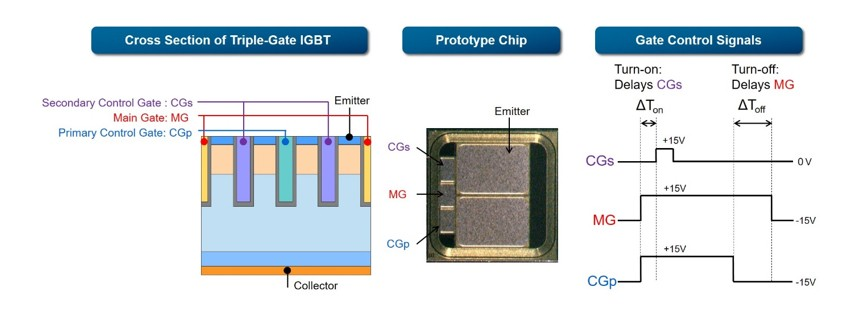
Toshiba has developed a triple-gate IGBT and gate control technology
that significantly reduces switching loss through flexible control of the accumulation of electrons and holes, from the gate drive circuit side.
The three gates,
the main gate (MG),
primary control gate (CGp),
and secondary control gate (CGs),
can be driven independently.
When gates are turned on,
delaying CGs and first turning on MG and CGp ensures simultaneous large electron and hole flows from the three gate electrodes,
and they accumulate in the IGBT at a higher speed, realizing a faster switching time and lower turn-on loss.
When turning the gates off,
electrons and holes inside the device are reduced by turning off CGp before MG, while leaving CGs off.
When the MG is switched off,
the IGBT switches off completely and the electrons and holes disappear at high speed, reducing turn-off loss.
Corporate Research & Development Center | Toshiba
https://www.global.toshiba/ww/technology/corporate/rdc/rd/topics/21/2106-01.html