东芝:开发三栅极IGBT:损耗降低40%
-三个栅电极减少了 40% 的开关损耗-
2021-06-02
东芝:
2021年6月2日,我们开发了“三栅极IGBT”。
IGBT(绝缘栅双极晶体管)是用于逆变器和DC-DC转换器等功率转换器的功率半导体。
与传统型号相比,开关电源时的损耗最多可减少 40.5%。
2023年至2024年的商业化:
今后,我们计划进行可靠性验证等实用化开发,并于2023年至2024年实现商业化。
在“ISPSD 2021”上宣布:
该研究成果将在功率半导体国际会议“ISPSD2021”(2021年5月30日至6月2日在线举行)上公布。
东芝研发中心
电子设备办公室总经理 Kazuto Takao 先生
他说,三栅极 IGBT“可以突破传统的性能饱和障碍”。
今日新闻
https://jp.rwwiki.cn/finances/57745.html
Toshiba’s Triple-Gate IGBT Power Semiconductors Cut Switching Power Losses by 40.5%
-Support high efficiency power converters for electrical systems and contribute to the realization of carbon-neutral economy-
2 June, 2021
Toshiba Corporation TOKYO─
Toshiba Corporation (TOKYO: 6502) has developed a prototype triple-gate IGBT*1
that reduces overall power loss by up to 40.5% when switching on and off (switching losses), the process of allowing and stopping electricity flow, in power semiconductors used to control electric power.
It is difficult to reduce power loss in IGBT,
due to a trade-off whereby reducing the loss when the IGBT is on (conduction losses) increases switching loss.
Toshiba took on this problem
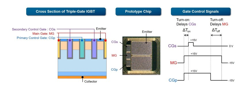
by developing a silicon IGBT with a new structure of three gate electrodes and gate control technology that delivers high accuracy gate electrode switching.
The new device
reduces turn-on loss*2 by 50% and turn-off loss*3 by 28%,
an overall reduction of up to 40.5% against a conventional single-gate electrode IGBT, with no increase in conduction losses.
The new technology is expected to boost the efficiency of power converters in electrical systems,
including renewable energy systems, electric vehicles, railroads, and industrial equipment.
Toshiba will present the technology at ISPSD2021, an international online conference from May 30 to June 3.
Toshiba has developed a triple-gate IGBT and gate control technology
that significantly reduces switching loss through flexible control of the accumulation of electrons and holes, from the gate drive circuit side.
The three gates,
the main gate (MG),
primary control gate (CGp),
and secondary control gate (CGs),
can be driven independently.
When gates are turned on,
delaying CGs and first turning on MG and CGp ensures simultaneous large electron and hole flows from the three gate electrodes,
and they accumulate in the IGBT at a higher speed, realizing a faster switching time and lower turn-on loss.
When turning the gates off,
electrons and holes inside the device are reduced by turning off CGp before MG, while leaving CGs off.
When the MG is switched off,
the IGBT switches off completely and the electrons and holes disappear at high speed, reducing turn-off loss.
Corporate Research & Development Center | Toshiba
https://www.global.toshiba/ww/technology/corporate/rdc/rd/topics/21/2106-01.html