東大:3D集積メモリを開発:フォンノイマンボトルネックを解決(動画):
Tokyo Univ: New 3D integrated memory: Solved the von Neumann bottleneck:
东京大学:开发3D集成内存:解决冯诺依曼瓶颈
ー高移動度トランジスタと、強誘電体キャパシタを同時集積ー
2021.06.01
東大と神戸製鋼:【記者発表】
◆強誘電体キャパシタを実現
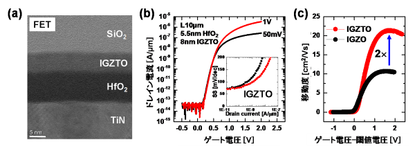
- Snを添加したIGZO材料を用いて、
- 移動度が従来に比べて2倍以上高いトランジスタと、
- 400℃以下の低温プロセスで形成可能な強誘電体キャパシタを実現しました。
◆3D集積メモリの動作実証
- 高移動度トランジスタと、
- 強誘電体キャパシタを同時集積して、
- 三次元集積可能なメモリデバイスの動作実証に成功しました。
◆機械学習をエッジデバイスにも実装
- このメモリデバイス技術により、
- 機械学習をエッジデバイスに実装することが出来、
- 人工知能を用いたより高度な社会サービスの展開が期待されます。
東京大学 小林准教授、
神戸製鋼所、
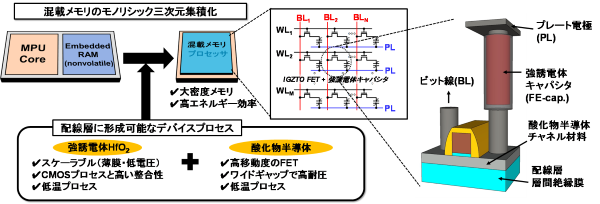
コベルコ科研、三次元集積メモリデバイスを開発:
Snを添加したIGZOを用いたトランジスタと、強誘電体HfO2キャパシタを集積し、
プロセッサの集積回路の配線層に混載可能なメモリデバイス技術の開発に成功しました。
従来の機械学習アルゴリズム:
機械学習アルゴリズムには、大容量メモリとプロセッサ-間の、効率的データ伝送が必要となります。
しかし、現在メインメモリは、プロセッサとは別チップで実装されています。
チップ間のデータ伝送効率が悪く、機械学習の計算処理が遅延します。
これをフォンノイマンボトルネックと呼びます。
フォンノイマンボトルネックを解決:
大容量のメモリと高効率なデータ伝送を両立するためには、プロセッサの集積回路の配線層に直接、三次元集積可能な混載メモリデバイスが有効な解決策となります。
プロセッサ配線層上に大容量メモリ:
プロセッサの配線層上に三次元集積できる大容量メモリを実現しました。
- プロセッサの直上に直接配線でき、
- データ伝送効率も向上、
- 機械学習の高エネルギー効率な実行、
上記2点が、可能となりました。
今回の成果:
機械学習を、高いエネルギー効率で計算出来ます。
エッジデバイスの性能アップ
エッジデバイスで、高度人工知能計算を行うことで、ビッグデータ・サービスの飛躍的な向上が期待されます。
東京大学生産技術研究所
https://www.iis.u-tokyo.ac.jp/ja/news/3569/
Closer hardware systems bring the future of artificial intelligence into view
Machine learning is the process by which computers adapt their responses without human intervention.
This form of artificial intelligence (AI)
is now common in everyday tools such as virtual assistants and is being developed for use in areas from medicine to agriculture.
A challenge posed by the rapid expansion of machine learning is the high energy demand of the complex computing processes.
Researchers from The University of Tokyo
have reported the first integration of a mobility-enhanced field-effect transistor (FET) and a ferroelectric capacitor (FE-CAP)
to bring the memory system into the proximity of a microprocessor and improve the efficiency of the data-intensive computing system.
Their findings were presented at the 2021 Symposium on VLSI Technology.
Memory cells require both a memory component and an access transistor.
In currently available examples, the access transistors are generally silicon-metal-oxide semiconductor FETs.
While the memory elements can be formed in the ‘back end of line’ (BEOL) layers,
the access transistors need to be formed in what are known as the ‘front end of line’ layers of the integrated circuit, which isn’t a good use of this space.
In contrast, oxide semiconductors such as indium gallium zinc oxide (IGZO)
can be included in BEOL layers because they can be processed at low temperatures.
By incorporating both the access transistor and the memory into a single monolith in the BEOL,
high-density, energy-efficient embedded memory can be achieved directly on a microprocessor.
The researchers
used IGZO doped with tin (IGZTO) for both the oxide semiconductor FET and ferroelectric capacitor (FE-cap) to create 3D embedded memory.
“The proximity achieved with our design will significantly reduce the distance that signals must travel, which will speed up learning and inference processes in AI computing, making them more energy efficient,”
study author Masaharu Kobayashi explains.
– Institute of Industrial Science, the University of Tokyo