東京エレクトロン:ASMLに提供:次世代EUV装置(動画):
Tokyo Electron: Provided to ASML: Next Generation Coater / Developer:
Tokyo Electron: 提供给 ASML: Next Generation Coater / Developer
東京エレクトロン:
6月8日、imec-ASML高NA EUV研究所に、次世代装置を供給する計画を発表した。
ASMLのEUV露光装置-次世代機に、組み合わせる。
東京エレクトロンは、
研究開発段階から、微細化技術世界トップ企業と組み、開発競争力を高める。
imec-ASML共同 EUV研究所:
東京エレクトロンが装置を供給するのは、imec-ASML高NA EUV研究所(フェルドホーフェン市)
半導体回路線幅の微細化技術R&Dで、世界トップレベルを誇る。
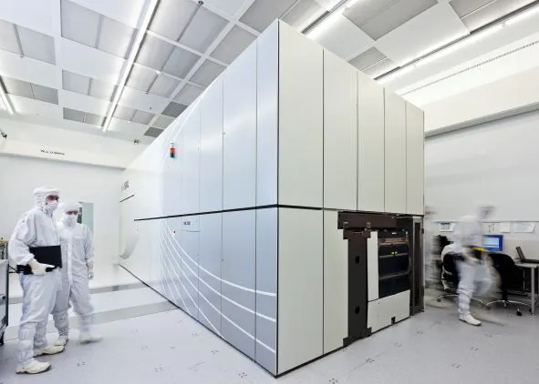
Coater/Developerを提供:
東京エレクトロンは、半導体にフォトレジストを塗布・現像するCoater/Developer(塗布現像装置)を提供する。
imec-ASML研究所に装置を出荷するのは初めて。
東京エレクトロンは、最先端半導体の研究開発に食い込むことで、競争優位性を高める。
東京エレクトロンの世界シェア:
調査会社グローバルネットによると、
- 東京エレクトロンは、Coater/Developerで、9割の世界シェア。
- 東京エレクトロンは 、EUV露光装置向けで、100%のシェア。
共同研究の目的:
- ASMLの次世代EUV露光装置と、
- 東京エレクトロンの塗布現像装置を、
- 統合・一体化させて、
半導体の生産性の向上を図る。
本格稼働時期:
東京エレクトロンの装置を2022年前半にも供給する。
組み合わせた装置は、2023年に稼働させる計画。
TSMCの採用時期:
現在TSMCは、「3ナノ製品」の開発を進めている。
TSMCは、2022年後半に「3ナノ製品」量産を開始する計画。
今回開発する次世代EUV露光装置は、この「3ナノ製品」以降の量産に適用する。
imecとの共同開発企業:
imecは半導体微細化に向けた研究に、力をいれている。
JSR
imecとの合弁会社で、EUV向けフォトレジストを生産する。大日本印刷(DNP)
imecと共同で、次世代半導体向けフォトマスクの開発を進めている。微細化技術の開発
EUV関連技術を持つASMLやimecなどとの協業が競争優位性を保つカギになる。日本経済新聞
https://www.nikkei.com/article/DGXZQOUC08CP10Y1A600C2000000/
Tokyo Electron to Collaborate with imec-ASML Joint High NA EUV Research Laboratory
Tokyo Electron announced today
the company will introduce its leading-edge Coater/Developer to the imec-ASML joint high NA EUV research laboratory in Veldhoven, the Netherlands.
The equipment
will be integrated inline* with EXE:5000, ASML’s next-generation high NA EUV lithography system with a 0.55 numerical aperture (NA), scheduled to be operational in 2023.
By collaborating with imec and ASML,
TEL will continue to pursue technological development to meet the ongoing scaling needs of its customers.
High NA EUV lithography
is expected to provide more advanced pattern scaling solutions compared to conventional EUV lithography.
The Coater/Developer being introduced to the joint high NA lab
will feature advanced capabilities which are not only compatible with widely used chemically amplified resists and underlayers,
but are also compatible with spin-on metal-containing resists.
Spin-on metal-containing resists
have demonstrated high resolution and high etch resistance, and are expected to enable finer patterning.
However, metal-containing resists
also require sophisticated pattern size control as well as metal contamination control on the backside and bevel of the wafer.
To meet these challenges,
the Coater/Developer being installed at the joint high NA lab comes with leading-edge process modules capable of handling metal-containing resists.
Combined with the new process modules, a single unit of TEL Coater/Developer
can process a wide variety of materials inline, including chemically amplified resists, metal-containing resists, and underlayers.
This will enable flexible fab operation, while also realizing increased productivity and high availability that are among the advantages of a Coater/Developer.
Yoshinobu Mitano, TEL Corporate Director, Senior Vice President and General Manager of SPE Business Division,
said,
“TEL is honored to collaborate with imec and ASML at the joint high NA lab to further understand and solve the challenges of high EUV NA patterning. By leveraging our experience in high volume manufacturing of EUV lithography process technology, we intend to deliver high NA EUV process solutions to our customers’ fabs in a timely manner.”
Notification | Tokyo Electron Ltd.
https://www.tel.com/news/topics/2021/20210608_001.html?_fsi=TmlRzK43