Taiwan TSMC: State-of-the-art microfabrication technology: Compared to China SMIC
Microfabrication technology: Roadmap
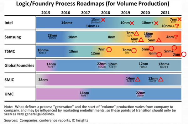
Figure 1 shows the roadmap for the world’s logic semiconductors and foundry microfabrication technologies.
Taiwan: TSMC’s cutting-edge technology
TSMC is at the forefront of microfabrication technology in the world.
In 2019, mass production of 7nm +, which applies the state-of-the-art exposure equipment EUV to holes, will be launched.
In 2020, we started mass production of 5nm with EUV applied to the wiring layer.
Risk production will begin in 2021.
Also, 3nm R & D is almost complete.
China: SMIC development status
On the other hand, the vulnerability of China SMIC has become apparent.
It will be miniaturized to 12 nm in 2019, 14 nm, and 2020.
However, it is hard to say that mass production has started in either case.
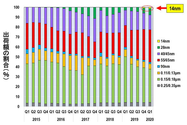
As shown in Fig. 2, the proportion of microfabrication technology in SMIC’s business is small.
SMIC: Q1 2020
This is because 14nm is only 1.3%.
At 12 nm, the ratio is zero.
Next, let’s consider what happens to 8-inch and 12-inch fabs if US-made manufacturing equipment cannot be introduced.
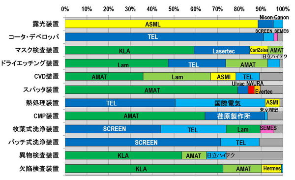
Supplier of semiconductor manufacturing equipment: Share by company
Figure 6 shows the share of various semiconductor manufacturing equipment by company in 2019.
It can be seen that most of the manufacturing equipment is oligopolized by one to three companies in Japan, the United States and Europe.
Under these circumstances, let’s consider the case where China SMIC is unable to introduce US-made manufacturing equipment.
Let’s check each of the various manufacturing equipment shown in Fig. 6.
Even if SMIC does not buy the equipment from the United States
If you buy from Japan / Europe, it may be possible to make 40nm or 28nm.
Procurement route for semiconductor manufacturing equipment:
Mask inspection device:
There is no problem if Japanese Lasertec sells the equipment instead of kLA.
Dry etching equipment:
If the insulating film etcher is introduced from Tokyo Electron (TEL) and the conductive film etcher is introduced from Hitachi High-Tech, it will be possible.
CVD equipment:
The presence of AMAT and Lam Research is extremely large. However, it may be possible to surpass it with European ASMI and TEL.
Sputtering device:
AMAT is the exclusive state of the sputtering equipment. It will be even more painful, but I have no choice but to use Japanese Ulvac or NAURA.
CMP device:
There is no problem if Ebara Corporation’s equipment is installed instead of AMAT.
Foreign matter inspection equipment and defect inspection equipment:
It’s quite painful that KLA cannot be used. However, Hitachi High-Tech and Hermes have no choice but to do something about it.
Looking at it this way, even without US-made manufacturing equipment
40nm seems to be manageable,
Isn’t 28nm quite painful?
However, if the equipment is introduced from Japan and Europe, it may be somehow manageable.
It can be said that it is a surprisingly good line that SMIC read that it took three years to realize 28 nm.
JBpress (Japan Business Press)
https://jbpress.ismedia.jp/articles/-/62312
Revenue per Wafer Rising As Demand Grows for sub-7nm IC Processes
Despite high development costs, using smaller nodes yield larger revenue per wafer