The new building at Osaka Works is due to be completed in the first half of FY2022.
( Source: Deposit Photos )

Sumitomo Chemical to Expand Photoresists
Business 27.04.2020
Sumitomo Chemical
has plans to strengthen the development and quality assurance system for photoresists for EUV lithography and other advanced semiconductor processes
due to the growing demand of photoresists in the market.
Japan – Sumitomo Chemical
has decided to construct a new building at Osaka Works and install new evaluation equipment, with the goal of strengthening the development
and quality assurance system for photoresists for EUV (extreme ultraviolet) lithography and other advanced semiconductor processes.
This project is due to be completed in the first half of FY2022.
Sumitomo Chemical to Strengthen Development and Quality Assurance System of Photoresists for EUV and Advanced Semiconductor Processes in Osaka Works
Apr. 22, 2020
Sumitomo Chemical
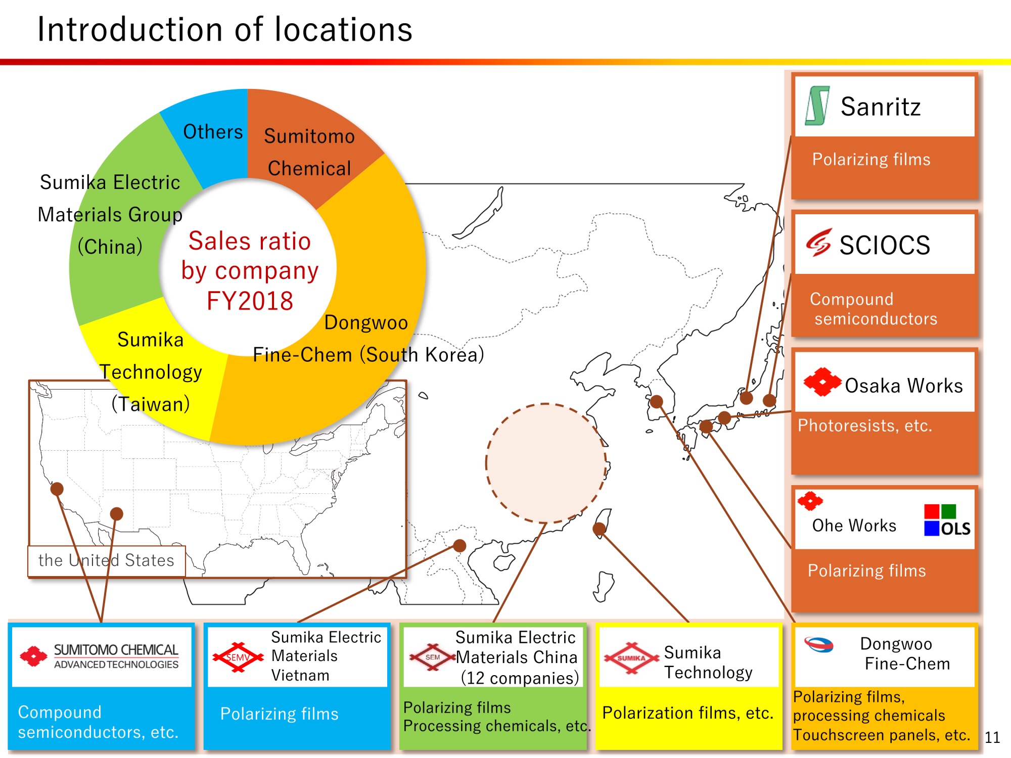
has decided to construct a new building in its Osaka Works (Konohana-ku, Osaka, Japan)
and install new evaluation equipment, with the goal of strengthening the development and quality assurance system for photoresists for EUV (extreme ultraviolet) lithography and other advanced semiconductor processes.
This project is due to be completed in the first half of FY2022.
Photoresists
are light-sensitive resin materials used in semiconductor photolithography processes.
Sumitomo Chemical has expanded its photoresist business by designing high-performance raw materials for photoresists and using its mass production technology,
while responding to customers timely through the integration of manufacturing, R&D, and sales functions in the Osaka Works.
To meet the bullish demand for photoresists,
Sumitomo Chemical
expanded production capacity for photoresists, of which it has a large market share in the world, for ArF (argon fluoride) immersion exposure in FY2019 by constructing a new plant in the Osaka Works.
In coming years, higher demand for the latest semiconductors is expected, against the backdrop of evolving
artificial intelligence (AI) technology and
the full-fledged commercialization of the next-generation communication system (5G).
In the cutting-edge semiconductor area,
EUV exposure, a new light source,
is expected to become a mainstream.
For its pattern formation,
photoresists suitable for further die shrink will be more in demand.
The company dramatically improved the performance of EUV photoresists by designing materials based on its unique concept and abundant knowledge it has cultivated to date.
The higher performance has been loudly cheered by customers and the company plans to mass-produce those high-performing EUV photoresists.
This structural enhancement is part of the company’s mid- to long-term plan to strengthen the operating base of the photoresist business for future growth.
By constructing a new building equipped with clean rooms and introducing new exposure equipment,
the company will increase its development efficiency of EUV photoresists and accelerate its response to customers while further enhancing the quality assurance system.
The company will also consider further investment in line with the future expansion of business in the cutting-edge photoresists area including EUV.
Sumitomo Chemical positions Information and Communication Technology (ICT) as one of the key areas in its Corporate Business Plan.
The company
will expand its portfolio in the entire semiconductor materials business by promoting growth of not only photoresists but also high-purity chemicals and compound semiconductor materials,
Business & Products | SUMITOMO CHEMICAL
https://www.sumitomo-chem.co.jp/english/news/detail/20200422e.html