Japan: Semiconductor devices and materials (post-process): Share ranking
-Competitiveness of “Japanese equipment and materials”-
Takashi Yunogami’s Nano Focus:
Last time, we discussed the front-end process / packaging.
About “things with a high market share in Japan”
We conducted an analysis of “its share, classification, and why?”
This time, we will discuss the post-process / package.
Paradigm shift with 3D ICs:
Finally, the era of three-dimensional packaging (3D IC) has arrived.
There is a paradigm shift between the pre-process and the post-process / packaging.
This will be pointed out below.
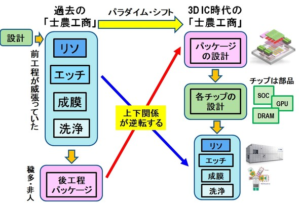
History of the paradigm shift:
1987-2002:
Writer-Takashi Yunogami was a microfabrication engineer from 1987 to 2002.
At that time, he was unaware of the back-end process and packaging.
2003-2008:
As a faculty member at Doshisha University, I investigated the post-process.
At that time, semiconductor processes had a clear hierarchy (Fig. 8).
Until around 2010:
The technician in the previous process was overwhelming.
Among them, lithography engineers reign supreme.
Modern Advanced Semiconductor Map:
However, the times have changed.
In modern advanced semiconductors,
Foundries such as TSMC,
Integrated Device Manufacturer (IDM) such as Intel and Samsung,
Outsourced Semiconductor Assembly and Test (OSAT),
Companies are competing to develop the latest 3D ICs.
Package development in 3D ICs:
In 3D ICs, the first thing to do is design the package.
Embedded parts in 3D ICs:
SoC (System on Chip),
GPU,
DRAM etc.
The “pre-process semiconductor chip” is no longer a “part”.
The elemental technology of the front-end process exists in order to manufacture the parts of the back-end process.
Post-process / packaging is noteworthy:
The “pre-process and post-process / package hierarchy” has been reversed.
as a result,
We have entered the “era when post-processes / packages are attracting attention”.
What is the “Japan share of post-process equipment and materials”?
Post-process and role of packaging:
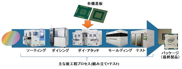
Figure 9 shows the outline of the post-process.
pre-process:
1000 chips are built on a silicon wafer.
It is individualized by dicing in the subsequent process.
Attached to the board material,
Various tests have been done,
Packaged and
The final product is completed.
The post-process is extremely complicated:
The reason why the post-process is more complicated than the pre-process is
This is because “the (mainly organic) substrate on which the chip is mounted differs depending on the application and company.”
in short,
“There is no world standard substrate like the silicon wafer in the front-end process in the back-end process.”
That makes it difficult to understand the post-process.
Post-process design rules are strict:
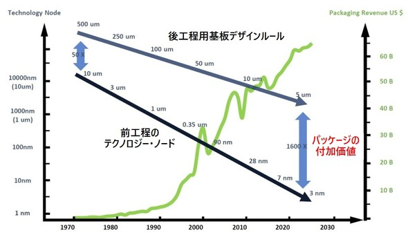
The design rules for the back-end process are three orders of magnitude larger than the technology nodes for the front-end process (Fig. 10).
in short,
In the previous process, TSMC is mass-producing 5nm.
The board design rule in the post-process is 5 μm.
Post-process / Importance of packaging:
The design rules for the post-process board are
If you follow the miniaturization of the previous process,
The final packaged product is ridiculously expensive.
“Here is the maximum added value of the post-process / package”.
“It’s not just about miniaturization.”
Share by company in post-process equipment:
Then, the share of substrate materials, substrates, post-process materials, and post-process equipment by company.
What is the position of the Japanese share?
-Share of substrate materials, substrates, post-process materials, post-process equipment-
Share of board materials by company:
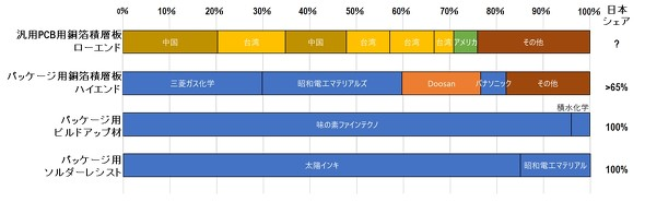
Figure 12 shows the market share of various substrate materials by company.
For low end:
-Copper foil laminated board for Printed Circuit Board
There is almost no share in Japan.
Chinese and Taiwanese manufacturers occupy the market share.
For high end:
-Copper foil laminated board for packaging
Japan’s share is over 65%.
Build-up board for packaging and
In the solder resist for packaging
Japan has a 100% monopoly.
Major board manufacturers in the world:
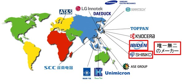
Figure 13 shows the major board manufacturers in the world.
Many board manufacturers are concentrated in Asia.
“Among them, IBIDEN and Shinko Denki of Japan” possess outstanding technology.
“Without these two companies, we can’t have a processor for servers.”
In short, “IBIDEN and Shinko Denki are unique”.
Share of post-process materials by company:
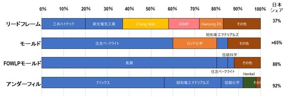
Furthermore, Fig. 14 shows the market share of various post-process materials by company.
Lead frame:
In “lead frame”, “Japan share is only 37%”.
Molding of sealing material:
However, it has a “65% share in Japan” for “molding of sealing materials”.
Mold material for FOWLP
InFO (Integrated Fan-Out WLP) developed by TSMC for iPhone.
“Molding material for FOWLP (Fan Out Wafer Level Packaging)” has “88% share in Japan”.
Underfill material:
In addition, “Underfill material” has a “Japan share of 92%”, which is also in a monopoly state.
Share of post-process equipment by company:
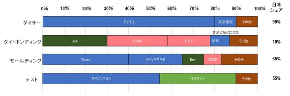
Finally, Fig. 15 shows the market share of various post-process equipment by company.
Dicer
In Dicer, Japan monopolizes 90% of the market share.
Die bonding
Die Bonding Japan share is only 10%,
65% in molding,
55% in the test,
Both are over half.
Japan’s competitiveness in the post-process:
in this way,
In substrate materials, substrates, post-process materials, post-process equipment,
“Overall, Japan has a high market share.”
It can be said that “Japan has great competitiveness in the world.”
For post-process / packaging
A source of competitiveness for equipment and materials
We analyzed Japanese companies that boast a high market share.
“Three points” emerge.
The first is:
Specializing in one material or device, he held down intellectual property.
There are companies that take an overwhelming share and keep other companies away.
for example:
Disco dicer (80%),
Ajinomoto Fine Techno Package Build-up Material (96%),
Solder resist (85%) for solar ink packaging, etc.
The second is:
Specializing in high-end products, developing world-class technology,
There are high-end companies that keep other companies away.
for example:
-For packaging copper foil laminates
Mitsubishi Gas Chemical (30%)
Showa Denko Materials (30%)
-For organic substrates
Ibiden and Shinko Denki’s organic substrates.
The third is:
Adopt a comprehensive approach with equipment, processes and materials.
There are companies that offer users multiple materials.
Showa Denko Materials:
A typical example of this is Showa Denko Materials.
Having a JOINT consortium has succeeded in supplying a large number of materials.
Sumitomo Bakelite:
Sumitomo Bakelite, which provides copper foil laminated boards and molding materials, is one of them.
Gain high market share in post-process / packaging:
In the post-process / package as well as in the pre-process
Serious and honest manufacturing of field engineers.
Japanese characteristics are the source of its competitiveness.
I speculated that Japanese ideas and behaviors are linked to a high market share.
–EE Times Japan
https://eetimes.itmedia.co.jp/ee/articles/2112/14/news034_3.html