
Adamant Namiki: Developed a 12-inch sapphire substrate!
– “Heteroepitaxial growth” is possible –
– 12-inch sapphire substrate for next-generation power semiconductors –
Adamant Namiki:
We have developed a sapphire substrate with a diameter of 12 inches (300mm).
“Heteroepitaxial growth”:
Gallium nitride and other substances different from sapphire
“Heteroepitaxial growth,” which grows on a substrate, is possible.
Installed in “automobiles, communication base stations, etc.”
Next-generation power semiconductors:
It can be used in the development of light-emitting elements such as micro light-emitting diodes (LEDs).
Development of sapphire substrate:
Namiki Adamant
2 inches (50 mm) in diameter,
4 inches (100 mm) in diameter,
6 inches (150 mm) in diameter,
8 inch diameter (200mm),
Developed and sold sapphire substrates.
12 inches is the maximum size.
Sapphire substrate:
It has the hardness second only to diamond, the hardest mineral.
Excellent heat resistance and corrosion resistance.
Substrate/Material
Contract processing service
Increase the sales of commissioned processing of substrates and materials including sapphire to 10 billion yen in five years.
(New Switch)-Yahoo! News
https://news.yahoo.co.jp/articles/ee16c39256849e5debfc4d19ec110a5083e05253
Adamant Namiki : a développé un substrat en saphir de 12 pouces !
– La “croissance hétéroépitaxiale” est possible –
– Substrat en saphir de 12 pouces pour les semi-conducteurs de puissance de nouvelle génération –
Namiki inflexible :
Nous avons développé un substrat en saphir d’un diamètre de 12 pouces (300 mm).
“Croissance hétéroépitaxiale”:
Nitrure de gallium et autres substances différentes du saphir
La “croissance hétéroépitaxiale”, qui se développe sur un substrat, est possible.
Installé dans “les automobiles, les stations de base de communication, etc.”
Semi-conducteurs de puissance de nouvelle génération :
Il peut être utilisé dans le développement d’éléments électroluminescents tels que les micro-diodes électroluminescentes (DEL).
Développement du substrat saphir :
Namiki Adamant
2 pouces (50 mm) de diamètre,
4 pouces (100 mm) de diamètre,
6 pouces (150 mm) de diamètre,
8 pouces de diamètre (200 mm),
Développé et vendu des substrats de saphir.
12 pouces est la taille maximale.
Substrat saphir :
Il a la dureté juste derrière le diamant, le minéral le plus dur.
Excellente résistance à la chaleur et résistance à la corrosion.
Substrat/Matériau
Service de traitement des contrats
Augmenter les ventes de traitement commandé de substrats et de matériaux, y compris le saphir, à 10 milliards de yens en cinq ans.
(Nouveau commutateur) – Yahoo Actualités
Adamant Namiki: Entwickelte ein 12-Zoll-Saphirsubstrat!
– “Heteroepitaxiales Wachstum” ist möglich –
– 12-Zoll-Saphirsubstrat für Leistungshalbleiter der nächsten Generation –
Adamant Namiki:
Wir haben ein Saphirsubstrat mit einem Durchmesser von 12 Zoll (300 mm) entwickelt.
“Heteroepitaxiales Wachstum”:
Galliumnitrid und andere von Saphir verschiedene Substanzen
“Heteroepitaxiales Wachstum”, das auf einem Substrat wächst, ist möglich.
Eingebaut in „Automobile, Kommunikationsbasisstationen usw.“
Leistungshalbleiter der nächsten Generation:
Es kann bei der Entwicklung von lichtemittierenden Elementen wie Mikro-Leuchtdioden (LEDs) verwendet werden.
Entwicklung des Saphirsubstrats:
Namiki Adamant
2 Zoll (50 mm) im Durchmesser,
4 Zoll (100 mm) im Durchmesser,
6 Zoll (150 mm) im Durchmesser,
8 Zoll Durchmesser (200 mm),
Entwicklung und Vertrieb von Saphirsubstraten.
12 Zoll ist die maximale Größe.
Saphirsubstrat:
Es hat die Härte, die nur von Diamant, dem härtesten Mineral, übertroffen wird.
Hervorragende Hitzebeständigkeit und Korrosionsbeständigkeit.
Untergrund/Material
Vertragsabwicklungsservice
Steigern Sie den Umsatz der Auftragsverarbeitung von Substraten und Materialien, einschließlich Saphir, in fünf Jahren auf 10 Milliarden Yen.
(Neuer Switch)-Yahoo!-Nachrichten
Adamant-Namiki employs a unique crystal growth method,
EFG (Edge-defined Film-Fed Growth Method), that eliminates the need for additional processing by growing single crystal sapphire in a sheet-shape,
thereby enabling the sapphire wafer to meet QCD (quality, cost, and delivery) requirements.
In addition to standard grade substrates for general LED use, we also offer high quality, prime grade wafers.
The high quality cleaning applied to prime grade wafers results in low particles and low metal contamination(*) .
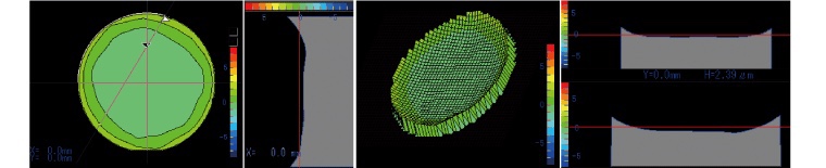
(*) K,Ca,Ti,Cr,Mn,Fe,Co,Ni,Cu,Zn < 5E10 /cm2 with TXRF We control flatness (TTV,BOW,WARP, etc.) with precision manufacturing technology,
and warpage problem that can occur during epitaxial growth is minimized.
The prime grade wafer is optimal for new process/product development.
Application examples of prime grade wafer:
micro-LED,
DUV-LED,
RF device,
AlN/Ga2O3 template.
High quality and services for next-generation semiconductor devices
and epitaxial growth
High flatness (controlled TTV, BOW, and WARP etc.)
High quality cleaning (low particles, lowmetal contamination)
Substrate drilling, grooving, cutting, and backside polishing
Attachment of measurement data such as cleanness and shape of substrate. (optional)
Depending on the specs, we have inventory for 2 to 8inch, or 300mm diameter substrates.
Please contact us for any inquiries.
Adamant Namiki Precision Jewel Co., Ltd.
https://www.ad-na.com/en/product/jewel/product/sapphire-wafers.html