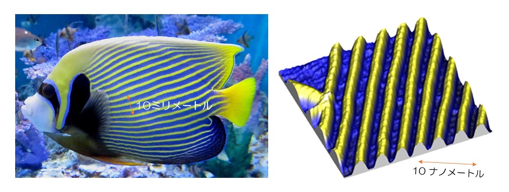
Tropical fish and nano-sized quantum wire patterns
Kyoto University/University of Tokyo: Fabrication of nano-quantum wires!
– Succeeded in fabricating 1 nm semiconductor quantum wires –
Graduate School of Kyoto University: Tomoya Asaba Program-Specific Associate Professor
University of Tokyo Graduate School: Professor Takatoshi Shibauchi
In collaboration with the University of Frankfurt, Germany, the research group has discovered a method for fabricating nano-quantum wires of ruthenium chloride (semiconductor) on a graphite substrate.
Fabrication of nano-quantum wires:
This quantum wire is extremely thin, with a thickness and width of 1 nm (several atoms), and a length of well over 1 μm.
It is possible to arrange the lines in a straight line at even intervals, and to change the width and spacing of the fine lines.
Such a quantum wire pattern is based on an unprecedented new mechanism.
Tropical fish stripes and giraffe mottling:
This quantum wire is the same principle as the striped pattern of tropical fish and the mottled pattern of giraffes.
The research group clarified that ‘it is likely to be formed spontaneously’.
This achievement provides a new perspective for nanotechnology ultra-fine processing.
It enables “fabrication of semiconductor and metal quantum wires of 1 nm”.
The results of this research were published in the US scientific journal Science Advances on May 4.
https://www.k.u-tokyo.ac.jp/information/category/press/10180.html
A quantum wire with a nano-level width created on the surface of a graphite substrate. A white round particle corresponds to a single ruthenium atom. (Provided by Kyoto University)
Fabrication of wires with a line width of several atoms: Application to 1nm semiconductors
Asahi Shimbun Digital reported:
Semiconductors are used in smartphones, cars, etc., and are essential to our lives.
In the current mainstream method, the surface of the substrate is shaved to fabricate the circuit.
Conventional line width/miniaturization:
It is extremely difficult to reduce the line width to 10 nm or less.
Even if the line width can be made ultrafine, it is difficult to create uniform and long circuits.
We have started mass production of next-generation chips with a line width reduced by 3 nm at our cutting-edge factories overseas, but we have seen the limits.
This new method:
It was vapor-deposited by irradiating a substance called ruthenium chloride on the surface of a graphite substrate with a laser beam.
Analyzed with a special microscope:
When the surface was observed at the atomic level, “a quantum wire with a line width of 1.4 nm corresponding to two ruthenium atoms” was formed.
The length of the quantum wire itself was 1,000 times its width.
By changing the vapor deposition time and substrate temperature, the width and spacing of the fine lines can be adjusted.
Various shapes such as striped patterns, X-shaped joints, Y-shaped joints, rings, and spirals are also possible.
Applications for “quantum circuits and atomic coils in addition to semiconductors” are conceivable.
https://www.asahi.com/articles/ASR5B6Q54R5BPLBJ004.html
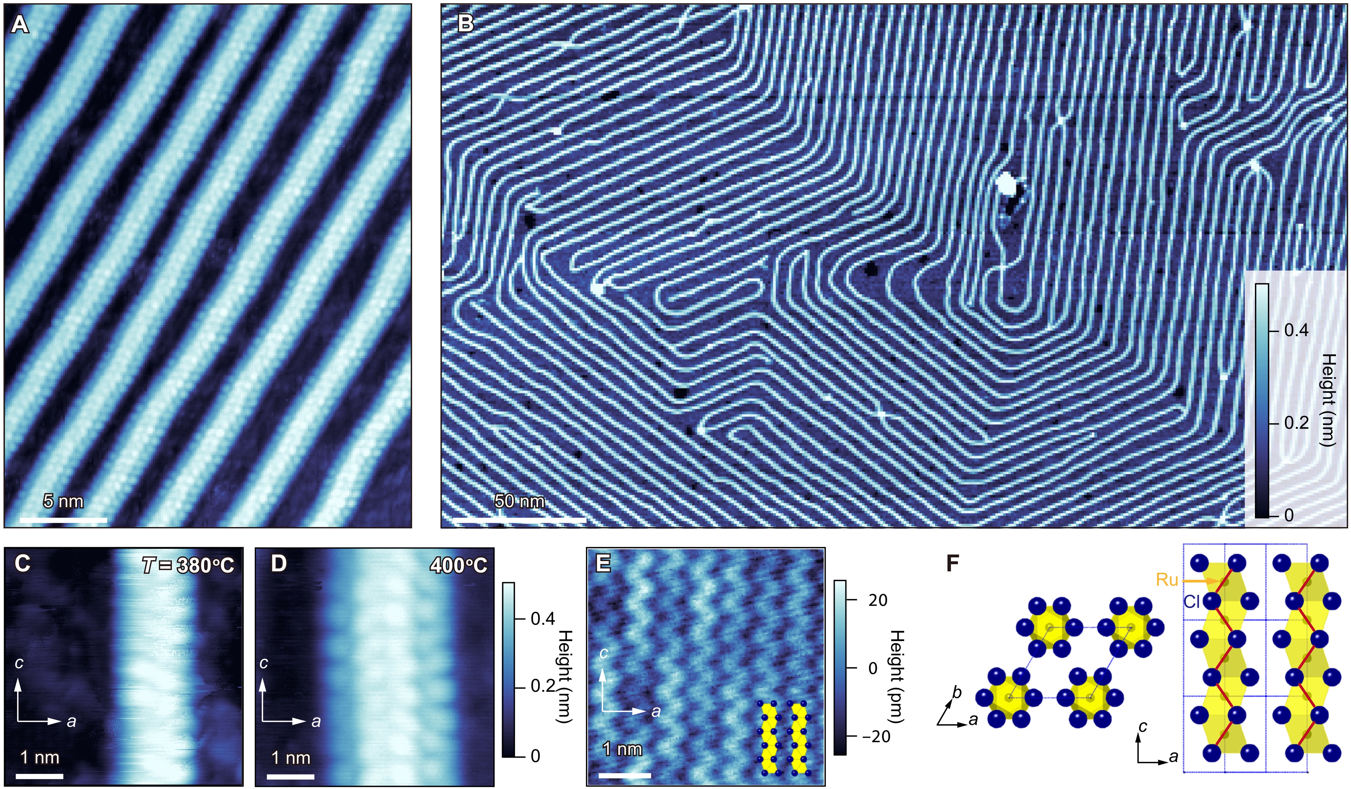
Fig. 1. Topographic images of β-RuCl3 atomic-scale wires grown on HOPG surfaces.
Growth of self-integrated atomic quantum wires and junctions of a Mott semiconductor
Abstract
Continued advances in quantum technologies rely on producing nanometer-scale wires.
Although several state-of-the-art nanolithographic technologies and bottom-up synthesis processes have been used to engineer these wires, critical challenges remain in growing uniform atomic-scale crystalline wires and constructing their network structures.
Here, we discover a simple method to fabricate atomic-scale wires with various arrangements, including stripes, X-junctions, Y-junctions, and nanorings.
Single-crystalline atomic-scale wires of a Mott insulator, whose bandgap is comparable to those of wide-gap semiconductors, are spontaneously grown on graphite substrates by pulsed-laser deposition.
These wires are one unit cell thick and have an exact width of two and four unit cells (1.4 and 2.8 nm) and lengths up to a few micrometers.
We show that the nonequilibrium reaction-diffusion processes may play an essential role in atomic pattern formation.
Our findings offer a previously unknown perspective on the nonequilibrium self-organization phenomena on an atomic scale, paving a unique way for the quantum architecture of nano-network.
https://www.science.org/doi/10.1126/sciadv.abq5561
Poissons tropicaux et motifs de fils quantiques nanométriques
Université de Kyoto/Université de Tokyo : Fabrication de fils nano-quantiques !
– Réussi à fabriquer des fils quantiques semi-conducteurs de 1 nm –
École supérieure de l’Université de Kyoto : professeur associé spécifique au programme Tomoya Asaba
École supérieure de l’Université de Tokyo : professeur Takatoshi Shibauchi
En collaboration avec l’Université de Francfort, en Allemagne, le groupe de recherche a découvert une méthode de fabrication de fils nano-quantiques de chlorure de ruthénium (semi-conducteur) sur un substrat en graphite.
Fabrication de fils nano-quantiques :
Ce fil quantique est extrêmement fin, avec une épaisseur et une largeur de 1 nm (plusieurs atomes), et une longueur bien supérieure à 1 μm.
Il est possible de disposer les lignes en ligne droite à intervalles réguliers et de modifier la largeur et l’espacement des lignes fines.
Un tel motif de fil quantique est basé sur un nouveau mécanisme sans précédent.
Rayures de poissons tropicaux et marbrures de girafe :
Ce fil quantique est le même principe que le motif rayé des poissons tropicaux et le motif marbré des girafes.
Le groupe de recherche a précisé qu ‘«il est susceptible de se former spontanément».
Cette réalisation offre une nouvelle perspective pour le traitement ultra-fin des nanotechnologies.
Il permet “la fabrication de fils quantiques semi-conducteurs et métalliques de 1 nm”.
Les résultats de cette recherche ont été publiés dans la revue scientifique américaine Science Advances le 4 mai.
https://www.k.u-tokyo.ac.jp/information/category/press/10180.html
Un fil quantique d’une largeur nanométrique créé à la surface d’un substrat en graphite. Une particule ronde blanche correspond à un seul atome de ruthénium. (Fourni par l’Université de Kyoto)
Fabrication de fils avec une largeur de ligne de plusieurs atomes : application aux semi-conducteurs 1nm
Asahi Shimbun Digital a rapporté :
Les semi-conducteurs sont utilisés dans les smartphones, les voitures, etc., et sont essentiels à nos vies.
Dans la méthode traditionnelle actuelle, la surface du substrat est rasée pour fabriquer le circuit.
Largeur de trait conventionnelle/miniaturisation :
Il est extrêmement difficile de réduire la largeur de ligne à 10 nm ou moins.
Même si la largeur de ligne peut être rendue ultrafine, il est difficile de créer des circuits uniformes et longs.
Nous avons commencé la production en série de puces de nouvelle génération avec une largeur de ligne réduite de 3 nm dans nos usines de pointe à l’étranger, mais nous avons vu les limites.
Cette nouvelle méthode :
Il a été déposé en phase vapeur en irradiant une substance appelée chlorure de ruthénium sur la surface d’un substrat en graphite avec un faisceau laser.
Analysé avec un microscope spécial :
Lorsque la surface a été observée au niveau atomique, “un fil quantique avec une largeur de ligne de 1,4 nm correspondant à deux atomes de ruthénium” s’est formé.
La longueur du fil quantique lui-même était de 1 000 fois sa largeur.
En modifiant le temps de dépôt en phase vapeur et la température du substrat, la largeur et l’espacement des lignes fines peuvent être ajustés.
Diverses formes telles que des motifs à rayures, des joints en forme de X, des joints en forme de Y, des anneaux et des spirales sont également possibles.
Des applications pour “des circuits quantiques et des bobines atomiques en plus des semi-conducteurs” sont envisageables.
Tropische Fische und Quantendrahtmuster in Nanogröße
Universität Kyoto/Universität Tokio: Herstellung von Nano-Quantendrähten!
– Erfolgreiche Herstellung von 1-nm-Halbleiter-Quantendrähten –
Graduiertenschule der Universität Kyoto: Programmspezifischer außerordentlicher Professor für Tomoya Asaba
Graduiertenschule der Universität Tokio: Professor Takatoshi Shibauchi
In Zusammenarbeit mit der Universität Frankfurt hat die Forschungsgruppe eine Methode zur Herstellung von Nano-Quantendrähten aus Rutheniumchlorid (Halbleiter) auf einem Graphitsubstrat entdeckt.
Herstellung von Nano-Quantendrähten:
Dieser Quantendraht ist extrem dünn, mit einer Dicke und Breite von 1 nm (mehrere Atome) und einer Länge von deutlich über 1 μm.
Es ist möglich, die Linien in gleichmäßigen Abständen geradlinig anzuordnen und die Breite und den Abstand der feinen Linien zu ändern.
Ein solches Quantendrahtmuster basiert auf einem beispiellosen neuen Mechanismus.
Tropische Fischstreifen und Giraffenflecken:
Dieser Quantendraht basiert auf dem gleichen Prinzip wie das Streifenmuster tropischer Fische und das gesprenkelte Muster von Giraffen.
Die Forschungsgruppe stellte klar, dass „es wahrscheinlich spontan entsteht“.
Diese Errungenschaft bietet eine neue Perspektive für die ultrafeine Verarbeitung der Nanotechnologie.
Es ermöglicht die „Herstellung von Halbleiter- und Metall-Quantendrähten von 1 nm“.
Die Ergebnisse dieser Forschung wurden am 4. Mai in der US-amerikanischen Fachzeitschrift Science Advances veröffentlicht.
https://www.k.u-tokyo.ac.jp/information/category/press/10180.html
Ein Quantendraht mit einer Breite im Nanobereich, der auf der Oberfläche eines Graphitsubstrats erzeugt wird. Ein weißes rundes Teilchen entspricht einem einzelnen Rutheniumatom. (Bereitgestellt von der Universität Kyoto)
Herstellung von Drähten mit einer Linienbreite von mehreren Atomen: Anwendung auf 1-nm-Halbleiter
Asahi Shimbun Digital berichtete:
Halbleiter werden in Smartphones, Autos usw. verwendet und sind für unser Leben unverzichtbar.
Bei der aktuellen Mainstream-Methode wird die Oberfläche des Substrats abgetragen, um den Schaltkreis herzustellen.
Konventionelle Linienbreite/Miniaturisierung:
Es ist äußerst schwierig, die Linienbreite auf 10 nm oder weniger zu reduzieren.
Selbst wenn die Linienbreite ultrafein gestaltet werden kann, ist es schwierig, gleichmäßige und lange Schaltkreise zu erstellen.
Wir haben in unseren hochmodernen Fabriken im Ausland mit der Massenproduktion von Chips der nächsten Generation mit einer um 3 nm reduzierten Linienbreite begonnen, aber wir haben die Grenzen gesehen.
Diese neue Methode:
Es wurde durch Bestrahlen einer Substanz namens Rutheniumchlorid mit einem Laserstrahl auf die Oberfläche eines Graphitsubstrats aufgedampft.
Mit einem Spezialmikroskop analysiert:
Bei der Beobachtung der Oberfläche auf atomarer Ebene entstand „ein Quantendraht mit einer Linienbreite von 1,4 nm, der zwei Rutheniumatomen entspricht“.
Die Länge des Quantendrahtes selbst betrug das Tausendfache seiner Breite.
Durch Ändern der Aufdampfzeit und der Substrattemperatur können Breite und Abstand der feinen Linien angepasst werden.
Auch verschiedene Formen wie Streifenmuster, X-förmige Verbindungen, Y-förmige Verbindungen, Ringe und Spiralen sind möglich.
Denkbar seien Anwendungen für „Quantenschaltungen und Atomspulen neben Halbleitern“.