AIST: SiC wafer mirror polishing speed increased by 12 times: for power semiconductors
-Significantly improved SiC wrapping process, which was difficult to speed up-
Development overview:
Mirror polishing of SiC wafers achieved 12 times faster than before
Solves the problems of frictional heat and abrasive grain breakage, which were problems in speeding up polishing
Batch polishing that processes multiple wafers at the same time greatly reduces processing time
National Institute of Advanced Industrial Science and Technology:
Mizuho Co., Ltd .:
Fujikoshi Machinery Industry:
We have developed a wrapping technology that achieves high-speed flattening of SiC wafers.
In particular, in the mirroring process, which was a low speed, a polishing speed 12 times faster than the conventional one was obtained.
It is comparable to the mirror grinding process of the sheet-style processing method.
Established a new batch processing technology.
Details of this technology:
It will be reported at the Academic Lecture Meeting of the Abrasive Grain Processing Society (ABTEC2021), which will be held online from September 1, 2021.
Reduction of SiC wafer manufacturing cost:
“Reducing the manufacturing cost of power element substrates and SiC wafers” is the most important factor in expanding the spread of SiC wafers.
Improved mass productivity of SiC wafer processing:
The SiC wafer processing process also requires high speed and parallel processing.
current problem:
Currently, the mass production efficiency of SiC wafers is poor.
SiC wafers are highly rigid and brittle materials that are extremely difficult to process.
Currently, SiC wafer flattening is performed by grinding or polishing.
Grinding
Grinding is a single-wafer type and mass production efficiency is poor.
Polishing
The polishing process is a batch method, and multiple sheets can be processed at once.
It takes more than 6 times as long as the number of processed sheets per unit time.
Efficient production technology is needed in the future:
The diameter of SiC wafers is increasing from 6 inches to 8 inches.
In the future, the scale of mass production will increase as the market expands.
We need processing technology that can produce SiC wafers more efficiently.
Conventional wafer flattening technology:
Polishing technology represented by wrapping and polishing
It is known as a batch processing technology suitable for mass production.
However, with batch processing technology,
Slurry may be cut due to the centrifugal force of the surface plate
There is a problem that it cannot be polished due to frictional heat,
The polishing speed could not be increased.
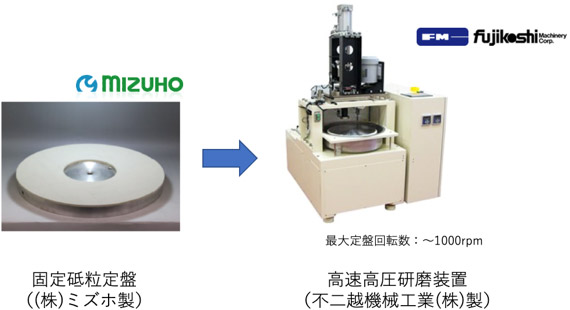
Developed a new diamond surface plate:
Therefore, a fixed abrasive grain surface plate obtained by molding a diamond grindstone into a surface plate was produced.
We tried to solve the problem by combining it with a high-speed polishing device.
Research results:
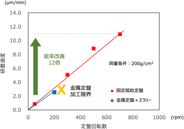
Conventionally, processing with a metal surface plate and slurry:
Processing using a metal surface plate and slurry became difficult at a surface plate rotation speed of over 200 rpm.
This time, processing using a fixed abrasive grain surface plate:
It was confirmed that the surface plate rotation speed and the polishing speed were proportional to each other even at 700 rpm.
Comparison result of old and new:
Comparisons were made under processing conditions using a slurry (load 200 g / cm2, rotation speed: 50 rpm).
The new method is 12 times faster than the old method.
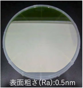
The Ra of the new fast-polished SiC wafer is 0.5 nm.
Achieves the same surface quality as conventional mirror grinding.
These results showed “the superiority of the combination of the fixed abrasive grain surface plate and the high-speed polishing device”.
https://www.aist.go.jp/aist_j/press_release/pr2021/pr20210831_2/pr20210831_2.html