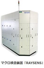
Tokyo Electron: Sales start of macro inspection device “RAYSENS”: Visual/sampling inspection automation
Tokyo Electron:
Announce date: June 9, 2020
-Automating visual inspection and sampling inspection to reduce inspection man-hours and stabilize wafer quality-
Device (TED):
We will develop the sales of “RAYSENS”, a macro inspection device that detects defects on the surface of compound semiconductor wafers at high speed and with high sensitivity.
Sold from June 9, 2020.
Nihon Keizai Shimbun
Macro inspection device: RAYSENS
Characteristic
Ultra-low noise macro optical sensor: Dedicated lighting detects wafer surface/small changes with high sensitivity
Dedicated optics, integrated software: High-efficiency transfer loader realizes high throughput
Transparent (semi-transparent) wafer: Wide range of inspections possible
Patterned, bare wafer: Both inspections possible
Dedicated integrated application: Device control, image capture, and judgment can be executed seamlessly
Assuming final appearance inspection: Wafer front/back surface/non-contact transfer inspection suppresses wafer back surface/contamination problem
Product Specifications:
Wafer size: 200 mm (open cassette compatible)
Pixel size: 7μm, 14μm, 28μm, 50μm
Lighting LED uniform line lighting
High intensity fiber lighting
Wafer transfer method
Conveyor loader specifications
Application Integrated control of optical unit,
Mechanical part integrated control,
Image scan,
Image processing function for macro inspection,
Defect detection judgment function
Ionizer
HEPA filter
inrevium|Tokyo Electron Device