Kyoto University: Doubled electron mobility of SiC-MOSFET: Significant improvement for the first time in 20 years
September 8, 2020,
Kyoto University:
Professor Kimoto and Dr. Tachiki: Research Group
Kyoto University has once again achieved a feat in research on SiC power semiconductors.
No thermal oxidation, no NO gas required, and oxide film formation was achieved.
SiC power semiconductor:
By a new method, oxide film formation
Reduces the defect density generated at the interface between SiC and SiO2,
Achieves twice the performance of the next,
This time, we made a prototype of n-type SiC-MOSFET.
Mr. Kimoto emphasized that it was a “breakthrough for 20 years.”
n-type SiC-MOSFET:
Conventional:
Point 2 and point 3 have been used alone so far, but neither has produced good results.
This method:
By using points 1 to 3 together, the interface defect density could be reduced.
Current method:
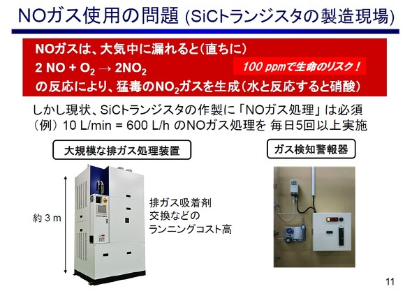
The interface is treated with NO (nitric oxide) to reduce defects that occur at the interface between SiC and SiO2.
NO is extremely toxic, and it costs a lot of money to procure NO, treat exhaust gas, and provide safety equipment.
Previous oxide film formation:
A Si thin film is deposited on a SiC wafer,
Thermally oxidize it at a low temperature of 750 ° C
Interfacial nitriding with nitrogen gas.
This approach:
Before forming the oxide film, the defects remaining on the surface of the SiC wafer are removed by hydrogen etching.
Depositing SiO2 on a SiC wafer by the CVD method without thermal oxidation to form an oxide film,
Nitriding the interface with nitrogen gas
Result of this time:
As a result of using this method, the interface defect density was reduced from the current 1.3 × 1011 cm-2 to 2.5 × 1010 cm-2, which is about one-fifth.
N-type and p-type SiC-MOSFET prototypes:
In the n-type, the electron mobility of SiC–MOSFET is doubled.
For the p type, a 1.5-fold performance improvement was confirmed.
In particular,
With n type, channel mobility has changed from 40 cm2 / Vs to 80 cm2 / Vs.
It is a p-type and has a channel mobility from 11 cm2 / Vs to 162 / Vs.
With a withstand voltage of 1200V class SiC-MOSFET, the on-resistance can be reduced by 25 to 35%.
In other words, the same rated current can be achieved with a chip size of 65 to 75%.
Device costs can be reduced by about 30% (Mr. Kimoto)
EE Times Japan