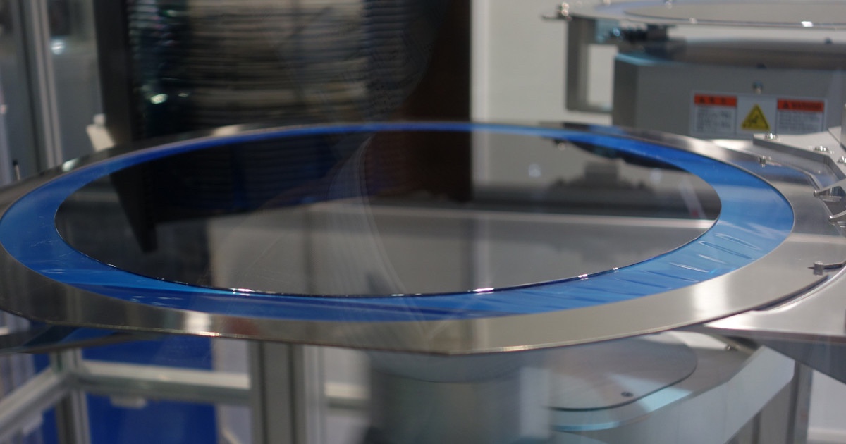
South Korea: Samsung’s semiconductor manufacturing crisis
-3nm GAA-Risk production: Yield rate is 10% to 20%-
Samsung:
Mass production of the next-generation standard 3nm is planned for the first half of 2022.
When risk production was carried out, the yield rate was 10% to 20%.
Reported by SBS Biz, a Korean medium.
Risk production:
Original trial production performed before ordering from a customer.
Samsung’s 3nm technology:
Developed GAA (Gate-All-Around) technology,
MBC FET (Multi-Bridge-Channel FET) technology is adopted.
Compared to 5nm EUV
Area reduced by up to 35%,
Performance improved by up to 30%,
It seems that power consumption is reduced by up to 50%.
Competitor GAA technology:
TSMC
It is used at 2nm, which is called N2.
Intel
It is adopted at 2nm called Intel 20A.
Samsung
Samsung is the first in the industry to adopt it.
Yield rate 10%:
10% of each wafer is standard compliant product and 90% is non-conforming product.
just,
The yield rate is 10% to 20% because 4nm in mass production is 35%.
It can be interpreted as excellent.
but,
Even with the old technology of 4 nm,
Since the yield rate does not exceed 50%,
Even if new technologies improve yield rates
The situation where many defective products occur remains unchanged.
Samsung’s 3nm technology is forced into tough production.
–ReaMEIZU
韓國:三星的半導體製造危機
-3nm GAA-風險生產:良率10%到20%-
三星:
下一代標準 3nm 計劃於 2022 年上半年量產。
進行風險生產時,收益率為10%~20%。
韓國媒體SBS Biz報導。
風險產生:
在客戶訂購之前進行的原始試生產。
三星的3nm技術:
開發GAA(Gate-All-Around)技術,
採用MBC FET(多橋通道FET)技術。
與 5nm EUV 相比
面積減少高達 35%,
性能提升高達 30%,
功耗似乎降低了 50%。
競爭對手GAA技術:
台積電
它用於2nm,稱為N2。
英特爾
它在 2nm 被採用,稱為 Intel 20A。
三星
三星是業內第一個採用它的公司。
收益率 10%:
每個晶圓的 10% 是符合標準的產品,90% 是不符合標準的產品。
只是,
良率是 10% 到 20%,因為 4nm 量產是 35%。
可以理解為優秀。
但,
即使採用 4nm 的老技術,
由於良品率不超過50%,
即使新技術提高了良率
很多次品出現的情況沒有改變。
三星的 3nm 技術被迫進入艱難的生產階段。
–瑞魅族